Open Nav


If you have ever opened up an electronic device—whether it is a smartphone, a computer, or a kitchen appliance—you have almost certainly interacted with a PCB. Yet for most people, the world of PCB assembly remains a complete mystery. Do not worry if terms like "surface mount technology" or "reflow soldering" sound like Greek to you right now. That is exactly what this guide is here to fix.
PCB assembly is the process of building the heart of every electronic device. Without properly assembled PCBs, the gadgets we rely on daily simply would not function. This article will walk you through every stage of the PCB assembly process in plain language, from the raw board arriving at a factory floor to the finished product that powers your favorite tech. By the time you finish reading, you will have a solid understanding of how electronics are actually made and why PCB assembly matters more than most people realize.
Before diving into assembly, it helps to understand what we are assembling in the first place.
A Printed Circuit Board (PCB) is a flat board made of insulating material—typically fiberglass (known as FR4) or composite epoxy—that mechanically supports and electrically connects electronic components using conductive pathways, pads, and other features etched from copper sheets. Think of it as the nervous system of an electronic device: it provides the physical framework and the electrical highways that allow components to communicate with each other.
PCBs come in several basic types:
The board alone is just a substrate with metal patterns. It becomes useful only after components are attached through the assembly process.
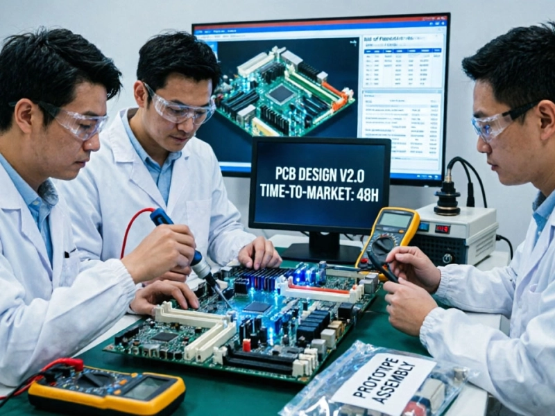
PCB assembly is where the magic happens. Even the most perfectly designed circuit board is useless without proper assembly. A single misplaced component or a weak solder joint can cause an entire device to fail. In high-reliability applications like medical devices, automotive electronics, or aerospace systems, a defect can have serious consequences.
The quality of PCB assembly directly impacts three key factors:
This is why electronics manufacturers invest heavily in assembly equipment, process control, and skilled technicians. The assembly line is where design meets physical reality.
The PCB assembly process consists of several distinct stages. Each stage has its own purpose, equipment requirements, and quality checkpoints. Here is a detailed breakdown.
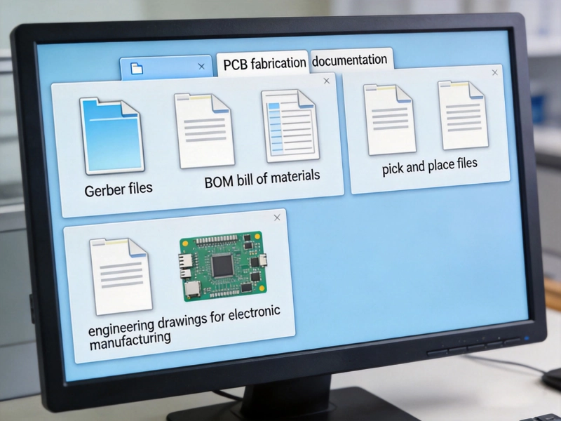
It all starts in a computer-aided design (CAD) software. Engineers use programs like Altium Designer, KiCad, or Eagle to create the schematic and board layout. The output is a set of Gerber files—the universal language of PCB manufacturing. These files contain all the information the assembly equipment needs: component placement coordinates, drill holes, solder mask layers, and paste stencil patterns.
Before any physical work begins, the design goes through Design for Manufacturability (DFM) review. This step catches potential issues early, such as component spacing violations, missing silkscreen labels, or footprints that do not match actual part dimensions. Catching a problem on paper costs pennies; catching it after assembly costs dollars.
PCBs are almost never manufactured one at a time. For efficiency, multiple boards are arranged in a larger panel—a rectangular array of identical boards with perforation or V-groove lines between them. Panelization allows the assembly line to process many boards simultaneously, reducing handling time and improving consistency.
This is where assembly truly begins. A thin stainless steel or nylon stencil is placed over the PCB panel, aligned precisely to match the solder pad locations. A squeegee spreads solder paste (a sticky mixture of fine tin-silver-copper alloy powder and flux) across the stencil, depositing it onto the pads in exactly the right amount.
Solder paste is temperature-sensitive and must be stored refrigerated. It is applied just before components are placed, and the stencil is cleaned and inspected between runs to ensure no paste buildup or misalignment.
Why it matters: Too much paste creates solder bridges between adjacent pads. Too little paste results in weak or open joints. The paste deposit is one of the most critical factors in assembly quality.
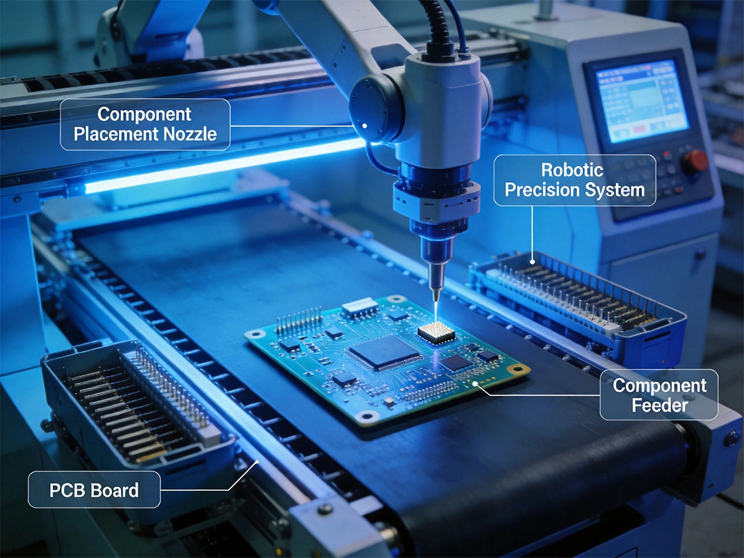
Once the paste is applied, the board moves to the pick-and-place machine—the star of any modern assembly line. These automated machines use vision systems and vacuum nozzles to pick components from reels, trays, or tubes and place them precisely onto the paste-covered pads.
Modern pick-and-place systems can place tens of thousands of components per hour with placement accuracy of ±0.05mm or better. They handle a wide variety of package types:
Some components are placed by hand in prototype runs or low-volume production, but automation is the standard for volume manufacturing because it is faster, more accurate, and more consistent.
After components are placed, the panel passes through a reflow oven—a multi-zone conveyor furnace that melts the solder paste and permanently fixes components to the board.
The reflow profile typically follows four temperature stages:
Each board profile must be optimized for its specific size, thickness, thermal mass, and component mix. Profiling is part science, part art, and getting it wrong leads to defects like tombstoning (when a component lifts off one pad like a tombstone), voids (gas bubbles in solder), or warped boards.
After reflow, every board goes through inspection. The sheer number of solder joints on a modern PCB—sometimes thousands per board—makes manual visual inspection impractical and unreliable. Instead, automated systems take over.
AOI (Automated Optical Inspection) uses high-resolution cameras and image processing algorithms to compare each board against a reference design. It can detect missing components, misaligned placements, tombstoning, insufficient or excess solder, and bridged connections. AOI works well for visible defects but struggles to see underneath components where solder issues can hide.
X-ray inspection is used for BGA (Ball Grid Array) packages and other components with hidden solder joints. X-rays penetrate the component body and reveal the solder beneath, detecting issues like voiding, head-in-pillow defects, and cold joints that optical systems cannot see.
ICT (In-Circuit Testing) applies electrical test signals to the board and verifies that each circuit node responds correctly. It can detect open circuits, shorts, and wrong component values. ICT requires test points added during design and a custom test fixture.
Not every board needs every test. The inspection strategy depends on the product's complexity, reliability requirements, and volume. A medical device board will go through far more rigorous testing than a cheap consumer gadget.
For boards that include through-hole components, there is an additional assembly stage. After reflow, through-hole parts are inserted either manually or with radial/axial insertion machines. The board then goes through wave soldering.
In wave soldering, the board is passed over a pump that creates a standing wave of molten solder. The bottom of the board contacts the wave, and solder wicks up through the holes by capillary action, creating strong joints on both sides. A nitrogen blanket is often used to reduce oxidation and improve wetting.
Some through-hole components are hand-soldered for rework or low-volume applications, though this is slower and less consistent than wave or selective soldering.
Many boards contain programmable components—microcontrollers, FPGAs, flash memory, or configuration resistors—that need to be programmed or configured before the board is finished. This may involve loading firmware, calibrating sensors, or setting unique IDs.
After programming, the board undergoes functional testing to verify it performs as designed. This might involve applying power, running diagnostic software, simulating input signals, and verifying outputs. Functional testing catches defects that electrical testing might miss, such as firmware bugs, sensor calibration errors, or intermittent issues.
For boards used in harsh environments—outdoor electronics, automotive under-hood applications, marine equipment—a conformal coating may be applied. This is a thin polymer film (acrylic, silicone, urethane, or parylene) that coats the board and protects it from moisture, dust, chemicals, and temperature extremes.
Coating is applied by spraying, brushing, dipping, or vapor deposition, and must cover the board uniformly without blocking connectors or test points. After coating, boards are often cured in an oven.
The last stage involves a final visual inspection, removal of any flux residue or contaminants (using ultrasonic cleaning, deionized water, or solvent-based cleaning), and packaging. Boards are packaged in anti-static trays, tubes, or reels depending on their form factor and shipped to the next stage of product assembly.
SMT is the dominant assembly technology today. Components are mounted directly onto the surface of the board without leads that go through holes. Advantages include:
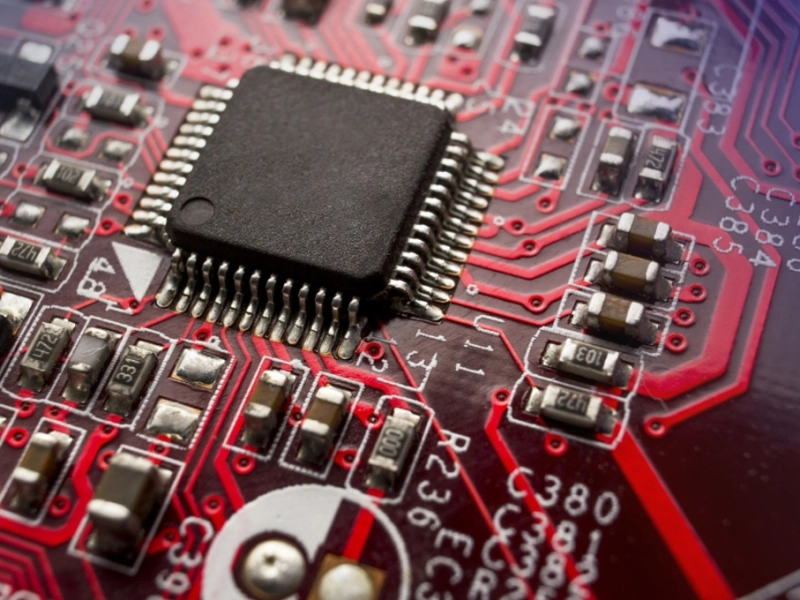
SMT components come in standardized packages like 0201, 0402, 0603 (imperial code referring to dimensions in hundredths of an inch), QFP (Quad Flat Package), QFN (Quad Flat No-lead), BGA, and many more. The trend is toward smaller packages as electronics get more compact.
THT uses components with leads that insert into holes and get soldered on the opposite side. While less common in volume production, it offers advantages for certain applications:
Examples include large electrolytic capacitors, transformers, heat sinks, and connectors in automotive and industrial equipment.
Most real-world products use a combination of SMT and THT. A consumer product might use SMT for most components (cost and space efficiency) while using through-hole parts for connectors, large power components, or mechanical mounting points. The assembly line must support both technologies, often requiring separate equipment and process steps.
Even with modern equipment and strict process controls, defects happen. Understanding common failure modes helps in both preventing them and diagnosing issues when they occur.
| Defect | Description | Common Causes | Prevention |
|---|---|---|---|
| Solder bridges | Unintended connection between adjacent pads due to excess solder | Too much paste, stencil misalignment, component shift during reflow | Proper paste deposit volume, stencil tensioning, optimized reflow profile |
| Cold joints | Dull, grainy solder joints with poor metallurgical bonds | Insufficient heat, contaminated surfaces, wrong solder alloy | Adequate reflow temperature and time, clean boards, nitrogen atmosphere |
| Tombstoning | Component lifts off one pad, standing vertically | Uneven paste on pad pairs, uneven heating, component size mismatch | Balanced paste deposition, proper thermal profiling |
| Voiding | Gas bubbles trapped in solder joints (especially under BGAs) | Rapid heating, outgassing from components or board | Controlled reflow ramp rates, pre-baking moisture-sensitive components |
| Lifted pads | Pad separates from board surface | Overheating, mechanical stress during rework | Careful rework technique, appropriate temperature limits |
| Component drift | Component ends up away from intended position | Pick-and-place feeder issues, vision system errors, insufficient paste | Regular feeder maintenance, board warpage correction, paste inspection |
| Head-in-pillow (HiP) | Partial joint separation between BGA and pad | Cooling too fast after reflow, board or component warpage | Controlled cooling, optimized reflow, proper board handling |
| Whisker growth | Tin whiskers causing short circuits | Pure tin plating, compressive stress, high humidity | Add lead to solder, reflow profile optimization |
Preventing defects requires a combination of good design practices (DFM), proper incoming material inspection, calibrated equipment, controlled processes, and statistical process monitoring. Many manufacturers use SPC (Statistical Process Control) to track key parameters like paste volume, placement accuracy, and reflow temperature in real time and trigger alerts when trends move toward out-of-spec.
If you are outsourcing your PCB assembly, whether for prototypes or production, selecting the right PCB assembly service is critical. Here are the factors that matter most.
Look for ISO 9001 (general quality management), ISO 13485 (medical devices), IATF 16949 (automotive), or AS9100 (aerospace) depending on your industry. These certifications indicate that the manufacturer follows documented quality processes, conducts regular audits, and maintains proper traceability.
Ask what testing they include in their standard assembly quote versus what costs extra. Common options:
Some assemblers specialize in prototypes and low-volume runs (10–100 boards) with quick turnaround. Others focus on high-volume production (10,000+ boards) with longer lead times but lower unit costs. Know your volume and timeline before approaching manufacturers.
A full-service assembler will source components on your behalf, leveraging relationships with authorized distributors to ensure authenticity and quality. This can save you significant time, but verify their supply chain practices—counterfeit components are a real industry problem.
Clear communication reduces errors. Ask about their process for handling design questions, deviations, or quality issues. Good assemblers provide detailed reports with each order, including inspection images, test results, and certificates of conformance.
PCB assembly technology continues to evolve rapidly, driven by demands for smaller, faster, and more reliable electronics.
Miniaturization is pushing the industry toward finer-pitch components, embedded components (where passives are buried inside the board layers), and advanced packaging like Chiplets—small, specialized chips that are assembled together like building blocks instead of a monolithic processor.
Automation is increasing with the adoption of Industry 4.0 principles: smart factories with IoT sensors, real-time data analytics, machine learning for defect prediction, and autonomous quality control. Digital twins of assembly lines allow engineers to simulate process changes before implementing them on the floor.
Sustainability is becoming a bigger factor, with regulations like RoHS (Restriction of Hazardous Substances) and REACH driving the adoption of lead-free solders, halogen-free materials, and recyclable packaging. Some manufacturers are exploring water-based cleaning processes and reduced energy consumption in reflow ovens.
Flexible and wearable electronics are creating new assembly challenges: how do you reliably mount components on flexible substrates that bend and flex during use? Specialized adhesives, strain-relief techniques, and novel interconnect materials are being developed to address these needs.
PCB assembly is the process of building a printed circuit board by attaching electronic components (like resistors, capacitors, and integrated circuits) to a bare PCB using soldering. It includes steps such as solder paste application, component placement, reflow soldering, inspection, and testing.
PCB manufacturing produces the bare board—the fiberglass substrate with etched copper traces and drilled holes. PCB assembly is what happens after: mounting and soldering components onto the manufactured board to make a functional circuit.
SMT stands for Surface Mount Technology. It is a method where components are mounted directly onto the surface of the PCB rather than being inserted through holes. SMT allows for smaller components, higher circuit density, and faster automated assembly.
A reflow oven melts solder paste to permanently attach surface mount components to a PCB. It uses a controlled temperature profile with multiple zones to gradually heat the board, melt the solder, and then cool it down in a controlled manner to form reliable solder joints.
It depends on the complexity and volume. Prototype runs of a few boards might take 3–7 business days. Standard production runs can take 2–4 weeks. High-complexity boards with advanced packaging or strict testing requirements may take longer. Rush services are often available at premium cost.
AOI stands for Automated Optical Inspection. It uses high-resolution cameras and image processing software to automatically inspect assembled PCBs for defects like missing components, misaligned parts, solder bridges, and insufficient solder.
Yes. Hand assembly is common for prototyping, low-volume production, repairs, and rework. It uses a soldering iron or hot air station to place and solder individual components. However, hand assembly is slow, less consistent, and impractical for fine-pitch components or high-volume production.
The most common lead-free alloy is SAC305 (96.5% tin, 3% silver, 0.5% copper) with a melting point of around 217°C. Lead-containing solders (typically tin-lead, Sn63Pb37) are still used in some applications where they are permitted, as they have a lower melting point and better wetting properties, but environmental regulations have pushed the industry toward lead-free alternatives.
PCB assembly is both a science and an art. It transforms raw materials and electronic components into the functional circuits that power the modern world. From the careful application of solder paste to the precision of pick-and-place machines, from the controlled heat of reflow ovens to the watchful eyes of automated inspection systems—every step matters.
Understanding the PCB assembly process gives you a deeper appreciation for the electronics around you and makes you a better informed buyer, designer, or engineer. Whether you are building your first hobby project, sourcing a prototype run, or scaling up for mass production, the principles covered in this guide will help you ask the right questions, avoid common pitfalls, and make better decisions.
The next time you pick up your phone or boot up your laptop, take a moment to think about the thousands of precisely assembled components and the carefully controlled processes that make it all work. The humble printed circuit board is one of the most remarkable manufacturing achievements of our time—and now you know exactly how it gets built.
What is Low Volume PCB Assembly?May/18/2026
Why Choose Low Volume PCB Assembly for Your Next Product Launch?July/02/2026
PCB Assembly FAQ: What Files Do I Need to Submit?June/17/2026
Accelerating Time-to-Market with Fast Prototype PCB AssemblyJune/10/2026
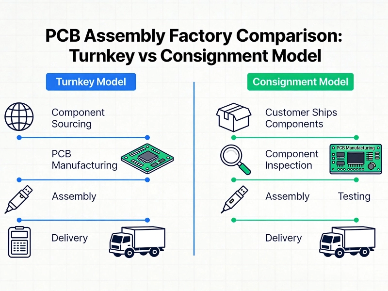
Turnkey PCB Assembly vs Consignment: Which Model Actually Fits Your Project?June/05/2026