Open Nav



If you've ever shipped a batch of PCBs only to have a customer call back about a short circuit you could have caught at the factory, you know exactly why inspection matters. Manual visual inspection works up to a point, but once production volumes climb past a few dozen boards, human consistency breaks down. Automated Optical Inspection (AOI) fills that gap — and in most modern SMT assembly lines, it has become one of the most important quality gates in the entire process.
This article explains how AOI actually works, where it sits in the production workflow, what it catches reliably, where it falls short, and how to interpret results in a way that drives real improvements rather than just generating defect logs.
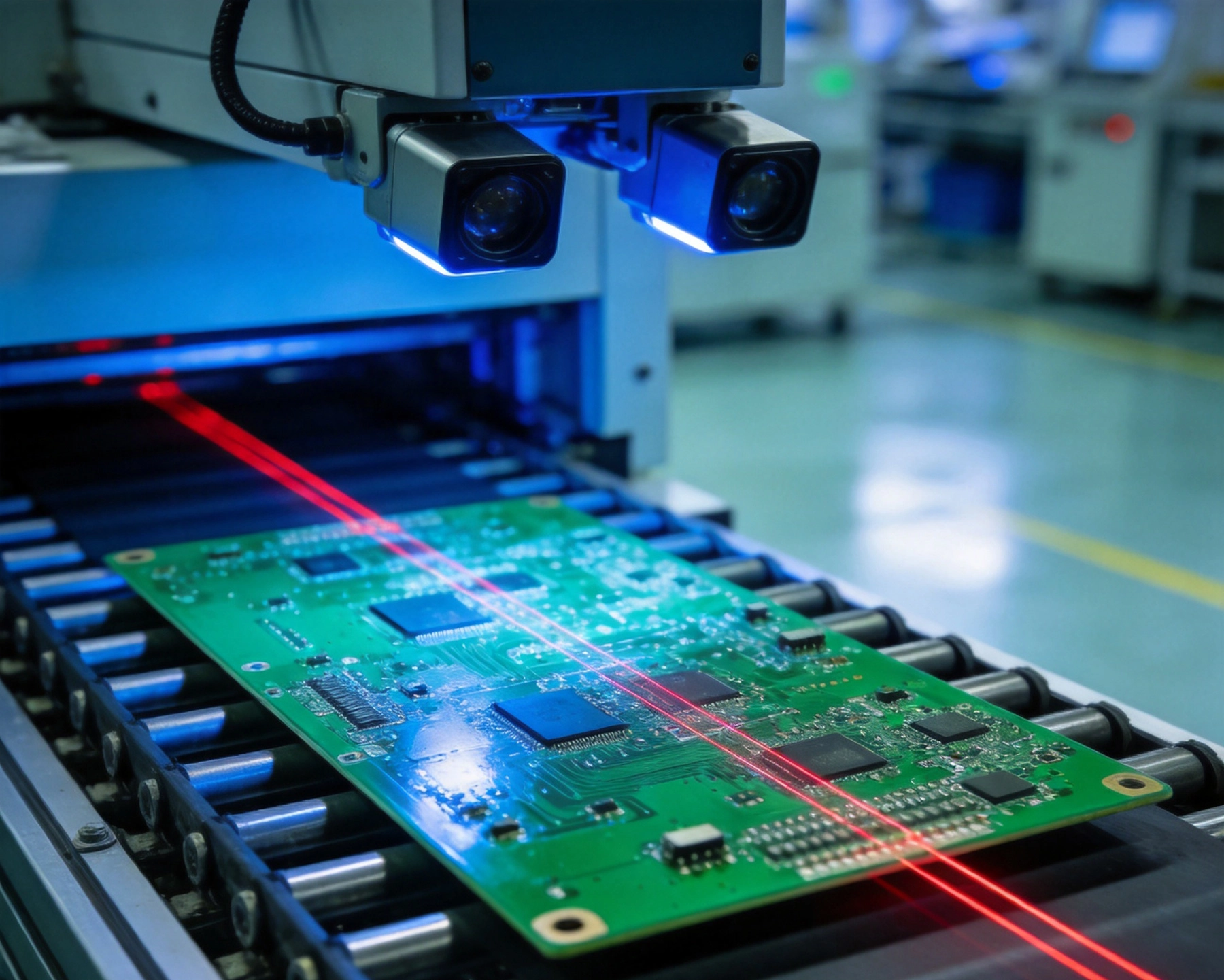
AOI stands for Automated Optical Inspection. It uses high-resolution cameras, structured LED lighting, and image processing software to examine a PCB at various stages of assembly. The system captures top-down images of the board, compares them against a known-good reference (the "golden board" or CAD data), and flags any deviations beyond the configured tolerance thresholds.
The cameras in an AOI system are typically arranged in multiple angles — overhead and oblique — to capture both the top surfaces of components and the side views of solder joints. Structured lighting at different colors and angles reveals defects that might be invisible under flat lighting: tombstoned components, insufficient solder, lifted leads, and coplanarity issues all show up differently depending on how the light hits them.
Modern AOI systems can operate in two modes. Reference-based inspection compares the board under test against a stored image of a known-good board. Rule-based inspection uses algorithmic criteria — minimum/maximum fillet height, acceptable land coverage percentages, component offset tolerances — without requiring a golden board image. Most production AOI systems blend both approaches, using rules for gross defects and references for fine alignment checks.
AOI is typically deployed at two critical points in the SMT assembly process. The first is after solder paste printing but before component placement. This is sometimes called pre-reflow AOI, and its job is to catch paste-related defects early — bridges, insufficient paste, offset prints. Catching these before components are placed saves the cost of the components themselves, which is the single biggest cost avoidance win in the entire inspection chain.
The second deployment point is post-reflow — after the board has gone through the reflow oven. Post-reflow AOI inspects the finished solder joints and component placement. It checks for missing components, misaligned parts, tombstoning, solder bridges, cold joints, and lifted leads. This is where the majority of AOI inspections happen, because by this point the board has all its components and the visual signature of a correctly assembled board is clearest.
Some assembly lines also run AOI after wave soldering for mixed-technology boards, inspecting the bottom-side thru-hole solder joints that reflow doesn't reach. Each additional inspection point adds cost and cycle time, so most manufacturers optimize around the two points above and only add more stages for high-reliability or high-cost applications where the risk justifies the overhead.
AOI is exceptionally good at finding defects that have a clear visual signature. In our production data across thousands of board builds, the categories AOI catches most consistently are:
AOI also generates quantifiable defect rate data across production runs. This statistical information is genuinely valuable — not just for rejecting bad boards, but for tracking process drift over time. If your AOI starts reporting a rising trend in tombstoning across three consecutive days, that's a process signal that can prevent an entire batch from going out of spec.
No inspection technology catches everything, and AOI has well-documented blind spots. The most significant is BGA and bottom-terminated components. When a BGA is placed and reflowed, all the solder joints are hidden underneath the component body. AOI cannot see them. X-ray inspection is the only optical-adjacent technology that can reliably detect BGA solder joint defects — voids, bridges, opens — without cross-sectioning the board. If your design includes BGAs, relying on AOI alone for those joints is a quality risk.
AOI also struggles with hidden solder joints under QFP leads that have shifted or lifted — the camera may catch the component misalignment but can't always confirm joint quality at the termination point. Similarly, voids within solder joints (trapped gas during reflow) are invisible to AOI since the surface can look completely normal while the internal structure is compromised.
Leadless components like MLCCs (multi-layer ceramic capacitors) are another area of reduced sensitivity. Hairline cracks in an MLCC body are almost impossible for AOI to detect reliably, yet they can cause field failures under thermal or mechanical stress. This is where flying probe testing, boundary scan, or functional test adds critical coverage that AOI alone cannot provide.
Finally, AOI's effectiveness depends heavily on library accuracy and programming quality. A poorly configured AOI system either generates excessive false positives (which creates unnecessary rework labor and cycle time) or misses real defects (which defeats the purpose). Getting the programming right — accurate pad definitions, appropriate threshold settings, correct lighting angles for each component type — takes time and engineering attention.
AOI and X-ray inspection are often discussed together, but they serve different purposes and are not interchangeable. AOI is fast (a typical board takes seconds to inspect) and economical for high-volume lines. X-ray is slower, more expensive per board, and requires specialized equipment and trained operators — but it sees inside packages.
The practical rule we use: AOI is your primary inspection workhorse for every board. X-ray is your targeted tool for high-risk joint categories — primarily BGAs, QFN packages with thermal pads, and any component where the solder joint is hidden from top-down view. Running X-ray on every board is cost-prohibitive for most production volumes, so X-ray inspection is typically reserved for qualification runs, first-article inspection, and failure analysis rather than 100% production screening.
Some manufacturers use AOI to sort boards, then apply statistical sampling with X-ray on boards flagged in high-risk areas. Others use X-ray as a 100% inspection for specific high-reliability product categories (medical, aerospace) where the cost of a field failure justifies the inspection overhead. The right approach depends on your defect landscape and your customer's quality requirements.
Running AOI without analyzing the data is like taking a temperature reading and calling it a diagnosis. The defect codes and locations that AOI reports are only useful when you track patterns over time and feed them back into process improvement.
The most valuable metric from AOI is defect per million (DPM) broken down by defect type. If you're seeing 800 DPM of tombstoning one week and 1,200 DPM the next, that's a process shift — and the likely cause is either paste degradation, stencil wear, or a change in the reflow oven profile. AOI logs make that correlation possible; without them, you're guessing.
Another useful analysis is defect location clustering. If all your opens and insufficient solder defects cluster in one corner of the board, that's a strong signal of a localized process problem — uneven paste release from that area of the stencil, a hotspot in the reflow oven, or a board design issue that creates a thermal anomaly during soldering. Clustered defects are almost always a process problem, not a component problem, and fixing the process is faster and cheaper than trying to rework individual boards.
We recommend reviewing AOI summary data at minimum weekly, and any time a new board design or component package enters production. This is also where close collaboration with your assembly partner pays off — a good contract manufacturer will proactively share AOI trends and suggest process corrections before your defect rate starts affecting outgoing quality.
If you're working with a new assembly partner or bringing up a new product, a few upfront steps make AOI significantly more effective from day one.
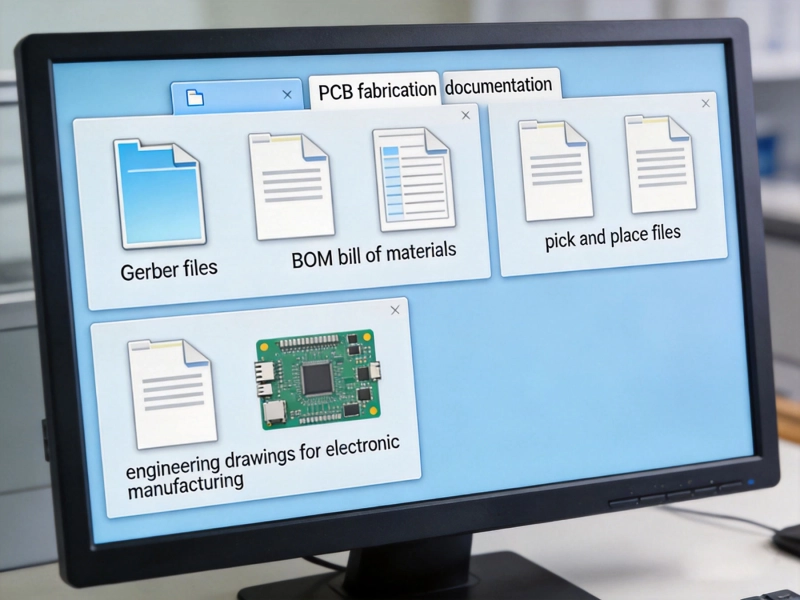
Share complete CAD and Gerber data upfront. AOI systems need accurate component position data, pad definitions, and polarity markings to program correctly. Sending incomplete data or mismatched files delays the AOI setup and increases the false-positive rate during the learning period.
Specify your critical component categories. Let your assembly partner know which packages or locations are highest risk for your application. This helps them configure lighting and thresholds appropriately — a connector that must not shift and a passive resistor that can tolerate minor offset should have different inspection criteria.
Discuss your accept/reject criteria before production starts. IPC-A-610 defines default criteria, but your application may need tighter tolerances in certain areas. Agreeing on these criteria upfront prevents friction during production and reduces the chance that a board gets routed to rework for a defect that doesn't actually affect function.
Request AOI data from the first production run. Even if you don't have the infrastructure to analyze it in-house, having that data available for review gives you visibility into what your boards actually look like. Any reputable assembly partner should be willing to share AOI logs and defect summaries on request.
For most consumer and commercial electronics, AOI combined with basic functional test provides solid quality coverage. But as product complexity increases, additional inspection and test layers become necessary.
Boundary scan testing (JTAG) addresses the hidden joint problem for complex ICs with many inaccessible pins. Flying probe testing applies electrical continuity and basic functional checks without requiring a custom fixture — useful for low-volume runs where fixture costs would be prohibitive. ICT (in-circuit test) provides comprehensive electrical verification of individual component values and circuit connectivity, but requires a custom bed-of-nails fixture that adds significant cost and lead time.
For high-reliability products — medical devices, automotive safety systems, aerospace electronics — the inspection and test regime typically includes AOI as the baseline, X-ray for hidden joints, ICT or flying probe for electrical verification, and functional or burn-in testing for end-item validation. No single technology covers everything. The combination that makes sense for your product is a function of the consequences of failure, the complexity of the design, and your production volume.
For production runs, AOI is far more consistent and thorough than manual inspection — a human inspector can maintain reliable attention for perhaps 20 minutes before error rates rise significantly. AOI doesn't fatigue. That said, AOI has blind spots (particularly hidden joints under BGAs), so a targeted manual inspection of those areas by a trained technician adds complementary coverage. The practical answer is that AOI eliminates routine manual inspection but does not eliminate human judgment for complex or ambiguous cases.
Partially. AOI can detect components that are the wrong size, wrong package type, or obviously mis-marked. What it cannot do is verify the internal quality of a component — the die inside an IC, the dielectric integrity of a capacitor, or the purity of a solder alloy. Component quality assurance requires incoming inspection, supplier qualification, and traceability programs that go beyond what AOI can inspect on the assembled board.
AOI adds roughly 3–8% to total assembly cost in our experience, depending on board complexity and the inspection configuration. This is a worthwhile investment for most production volumes because the cost of catching and reworking a defect at the factory is a fraction of the cost of a field failure. For very high-volume, very simple boards (single-sided, large pad pitch, low component count), the economics are tighter and some manufacturers skip AOI in favor of statistical process control — though this carries risk.
A well-configured AOI system running on a mature product typically achieves defect detection rates above 90% for visually detectable defects. The escape rate (defects that pass through AOI undetected) varies by defect type: AOI catches almost all gross defects like missing components or large bridges, but has lower sensitivity for fine-pitch defects and hidden joints. The combined inspection and test regime — AOI plus X-ray plus functional test — should achieve overall escape rates well below 1% for most commercial applications.
Ask three specific questions: What AOI system do they use, and is it regularly calibrated? What are their typical false-positive and false-negative rates on similar board complexity? And can they share AOI defect data from recent production runs? If they can't answer these questions confidently, that's a signal that their quality program may not be as mature as their sales pitch suggests. A credible assembly partner should be transparent about their inspection capabilities and happy to show you their process data.
What's the Difference Between Prototype PCB Assembly and Low Volume PCB Assembly ?May/18/2026
Prototype PCB Assembly Explained: Why It's Crucial for R&DJuly/14/2026
Turnkey PCB Assembly vs Consignment: Which Model Actually Fits Your Project?June/05/2026
PCB Assembly FAQ: What Files Do I Need to Submit?June/17/2026
What Are the Benefits of Small Batch PCB Assembly?May/18/2026