Open Nav



Surface Mount Technology has fundamentally reshaped how electronic circuits are built. Where once engineers threaded components through holes in circuit boards by hand, today's SMT PCB assembly lines move with extraordinary precision and speed—placing hundreds of thousands of components per hour with tolerances measured in microns. Understanding this process isn't just for manufacturing engineers; product designers, hardware founders, and procurement teams benefit enormously from knowing exactly what happens inside an assembly facility.
This article walks through each stage of the SMT assembly process in sequence, explaining what happens at each step, why it matters, and what quality considerations guide the journey from bare board to finished product. Whether you're sending your first board out for assembly or looking to optimize an existing production flow, a clear understanding of the SMT assembly line demystifies one of the most consequential stages in electronics manufacturing.
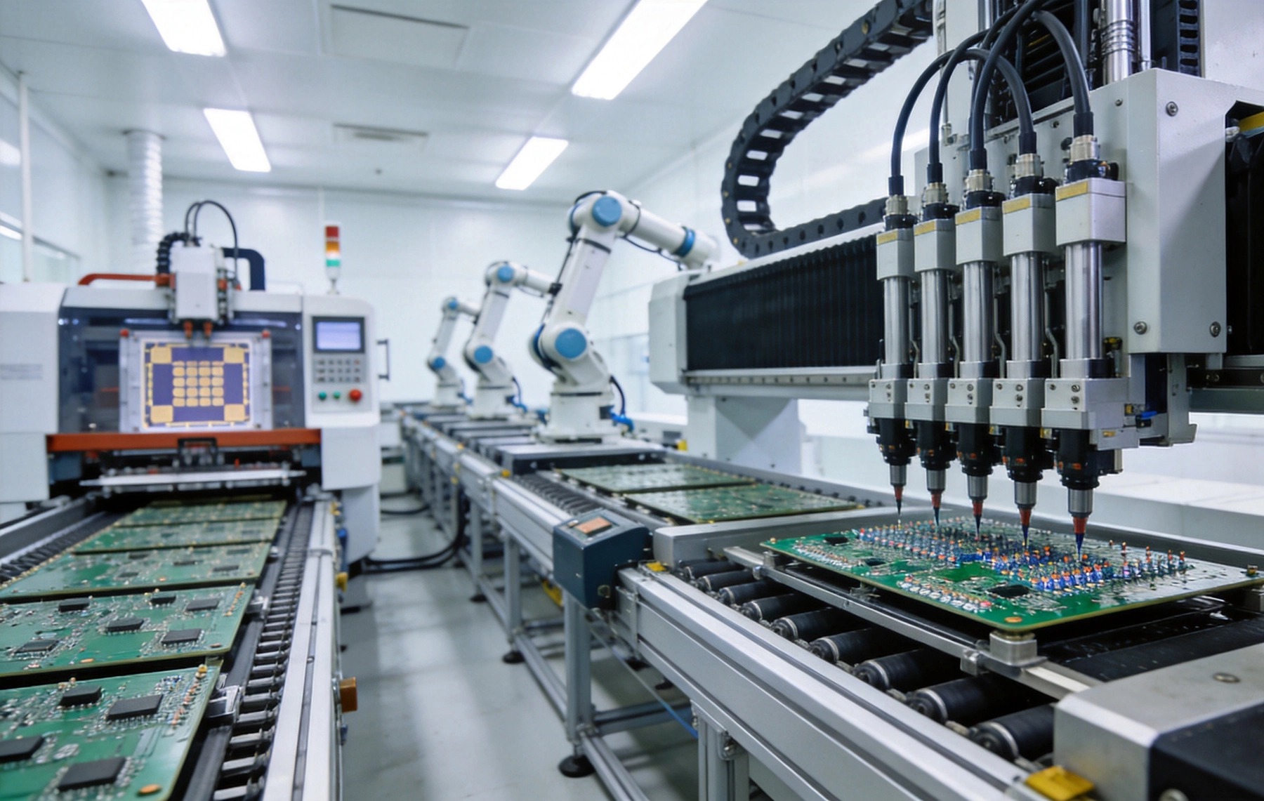
The journey of a PCB through the assembly line begins with solder paste—a sticky mixture of fine metal solder particles suspended in flux, formulated to hold components in place before reflow soldering locks them permanently. The paste is applied to the bare board through a precision stencil, a thin metal sheet laser-cut to match exactly the pad pattern of the PCB design.
A skilled stencil printer deposits the correct amount of paste on every pad simultaneously. The machine's squeegee blades push the paste across the stencil openings under controlled pressure and speed, filling each aperture before lifting away to leave a precise deposit. Modern printers use optical recognition systems to align the stencil perfectly with the board, compensating for any panel bow, board warp, or stencil misalignment before the printing cycle begins.
The quality of solder paste printing determines everything that follows. Too little paste produces weak solder joints prone to failure under thermal or mechanical stress. Too much paste causes bridging—unintended connections between adjacent pads that create shorts and functional failures. The paste deposit must be uniform, consistent across the board, and precisely aligned with pad locations. Automated optical inspection immediately following printing catches defects before they propagate through subsequent stages, saving costly rework downstream.
Stencil thickness and aperture design are engineering decisions that directly impact assembly quality. Thicker stencils deposit more paste, appropriate for large pads, while finer apertures require thinner stencils to achieve acceptable paste release. Laser-cut stencils with electropolished apertures provide the best paste transfer efficiency for modern fine-pitch components. Nano-coatings on stencil surfaces further improve release characteristics, reducing the defects that plague poorly maintained equipment.
Once the board exits the printer carrying its load of fresh solder paste, it enters the most visible and technically impressive stage of the assembly line: the pick-and-place machine. Here, high-speed robotic heads lift surface mount components from feeders arranged in precision racks and position them onto the paste-coated pads with remarkable accuracy—typically within 50 microns for standard components, and tighter still for fine-pitch devices.
Modern placement machines operate at remarkable speeds. High-volume lines place 30,000 to 80,000 components per hour, while precision placers sacrifice raw speed for greater accuracy when handling challenging parts like fine-pitch BGAs, 01005 resistors, or large QFP packages. Most production lines use a combination: a fast bulk-placer for standard passive components and a precision-placer for complex ICs and sensitive parts.
The machine's vision system plays a critical role in placement accuracy. Before picking each component, the machine photographs the part from multiple angles to verify orientation, check for damaged or missing parts, and adjust pick-up position for any misalignment. After placement, a second camera confirms the component landed correctly before the board moves forward. This closed-loop verification catches errors in real time rather than discovering defects after reflow.
Not all components place easily. Tape-and-reel packaging works smoothly with standard feeders, but loose parts in trays, tubes, or cut tape require different handling approaches. Moisture-sensitive devices like BGA and QFN packages must be handled according to strict floor life rules—exposure to humidity above specified thresholds risks delamination or popcorn cracking during reflow. Experienced assembly facilities track component moisture sensitivity levels and manage assembly schedules to prevent moisture damage.
With all components placed onto the paste-coated board, the assembly moves into the reflow oven—a carefully controlled furnace that melts the solder paste to create permanent electrical and mechanical connections. The board travels through the oven on a conveyor belt, passing through a series of temperature zones programmed to follow a precise thermal profile.
The reflow profile typically includes four phases. First, a preheat zone gradually raises the board temperature to avoid thermal shock, activating the flux in the solder paste to clean oxide contamination from pad and component termination surfaces. Second, a soak zone holds temperature stable to equalize thermal mass across the board and complete flux activation. Third, the reflow zone peaks above the solder's liquidus temperature, melting the solder and forming metallurgical bonds with the component leads and PCB pads. Finally, a controlled cooldown solidifies the joints without introducing thermal stress that could crack brittle connections.
Profile optimization is both science and art. Each board stackup—thickness, copper weight, component density—creates a unique thermal environment. Dense boards with large BGAs absorb less heat per unit area than simple two-layer boards with mostly passive components. Profiling engineers use thermocouples bonded to representative boards to characterize thermal behavior and fine-tune zone temperatures, belt speed, and dwell times until the profile achieves the correct peak temperature and time above liquidus for reliable joint formation.
Even well-designed processes produce occasional defects. Tombstoning—where a component stands up on one end like a tombstone—results from uneven wetting forces, often caused by uneven paste deposits or components landing off-pad. Head-in-pillow defects occur when BGA spheres don't fully merge with paste deposits, creating partially connected joints that pass initial testing but fail under thermal cycling. Cold joints from insufficient peak temperature produce dull, granular joints prone to mechanical failure. Each defect points to specific process or material issues that process engineers must diagnose and resolve.
After reflow, the board moves through inspection stages that identify defects before they reach customers. The sheer volume of solder joints on a modern assembly—potentially thousands per board—makes manual inspection impractical. Automated inspection systems fill this role with far greater consistency and coverage.
Automated Optical Inspection uses high-resolution cameras and sophisticated image analysis software to examine every visible joint for defects: missing components, misaligned placements, insufficient solder, bridging, tombstoning, and countless other failure modes. The system compares each inspection point against both a golden reference board and library-based defect criteria, flagging anomalies for operator review. AOI catches most defect types effectively but struggles with hidden joints under BGAs or other bottom-terminated components.
X-ray inspection addresses the blind spots in optical inspection. By penetrate through materials invisible to optical cameras, X-ray systems reveal the internal structure of solder joints, checking for voids in BGA joints, misaligned BGA spheres, and other hidden defects. High-volume facilities use X-ray inspection selectively on high-reliability products or boards with known risk profiles, while critical applications like automotive and medical electronics may require 100% X-ray inspection of BGA assemblies.
Electrical testing complements visual inspection by verifying functional connectivity rather than just physical appearance. Flying probe testers use spring-loaded pins that make temporary contact with test points on the board, measuring resistance and capacitance to verify network continuity and isolation. While slower than bed-of-nails fixture testing, flying probe requires no custom fixture, making it ideal for prototype quantities and small batches where fixture costs would be prohibitive. The combination of AOI, X-ray, and electrical testing provides overlapping coverage that catches virtually all significant defects.
Not all components attach to surface mount pads. Through-hole components—connectors, electrolytic capacitors, large inductors, and many connectors—require leads inserted through holes in the board and soldered on the opposite side. When assemblies include both SMT and through-hole components, the assembly line must accommodate both technologies.
The most common through-hole assembly method on mixed-technology boards is selective soldering, which applies solder only to through-hole leads without reflowing the entire board. A programmable nozzle dispenses a controlled solder wave exactly where needed, while masked areas of the board prevent solder from reaching unintended locations. Selective soldering handles most mixed-technology assemblies efficiently and avoids the equipment cost and thermal stress of full wave soldering.
For higher-volume production, wave soldering remains the standard approach. The board passes over a pump-generated wave of molten solder that contacts the bottom of the board, wicking up through the holes to create joints. Wave soldering requires careful process control—flux application, preheat, solder temperature, conveyor angle, and contact time all affect joint quality—but achieves throughput rates impossible with selective soldering. The choice between selective and wave soldering depends on production volume, board complexity, and the specific component mix on each assembly.
After soldering, residual flux and other contaminants remain on the board surface. For most applications, the residue left by no-clean flux formulations is acceptable and requires no additional cleaning. However, high-reliability applications—automotive under-hood electronics, aerospace systems, and many medical devices—require thorough cleaning to remove all traces of ionic contamination that could cause dendritic growth and eventual failure under humidity and voltage stress.
Board cleaning uses aqueous cleaning systems or solvent-based processes depending on residue characteristics and board construction. Aqueous systems spray heated deionized water or specialized cleaning solutions across the board surface, flushing away contamination. Critical boards may undergo multiple wash cycles with rinses to ensure complete contaminant removal. After cleaning, boards must be dried thoroughly—moisture trapped under components creates reliability risks equivalent to the contamination being removed.
Conformal coating provides additional protection for boards operating in harsh environments. This thin polymer film—typically acrylic, urethane, or silicone—conforms to the board topology, sealing components and traces against moisture, dust, and chemical exposure. Boards designated for conformal coating must be cleaned before coating, as trapped contamination accelerates coating delamination and creates reliability failure modes. Application methods include spray coating, dip coating, and selective robotic coating for partial coverage.
The final stage of the assembly line represents the last opportunity to catch defects before shipment. Final visual inspection verifies that cleaning, coating, and any hand-soldered rework left the board in acceptable condition. Inspectors check for damaged components, scratched boards, coating defects, and any cosmetic issues that might indicate underlying problems.
Functional testing validates that the assembled board performs its intended function. In-circuit testing checks individual circuit nodes against expected values, verifying that every component is present, correctly placed, and functioning within tolerance. Functional system tests power up the board and exercise its operating modes, verifying that the complete assembly behaves as designed. Flying probe, fixture-based in-circuit test, and functional test each play roles depending on board complexity and quality requirements.
Boards that pass all inspections and tests move to pack-out, where they are carefully packaged to survive shipment. Anti-static bags protect against electrostatic discharge. Foam or bubble wrap cushions prevent mechanical shock. Humidity indicator cards show whether moisture entered packaging during transit. For high-value assemblies, tracking and chain-of-custody documentation ensures accountability through the logistics chain. The journey from bare board to shippable product completes when properly packaged assemblies leave the facility.
Beneath the physical assembly process runs a parallel track of preparation work that determines whether the line produces good boards or endless defects. This invisible process includes Gerber file review, assembly drawing creation, stencil design, feeder setup, pick-and-place program development, reflow profile development, test program creation, and first-article inspection protocols.
Gerber file review verifies that manufacturing data is complete, internally consistent, and suitable for production use. Missing drill files, misaligned layers, and clearance violations caught during review prevent line stoppages and defective boards. The review process also identifies opportunities to optimize panel utilization and reduce material waste—decisions that affect cost and delivery as much as quality.
First-article inspection marks the transition from setup to production. The initial board produced on a new job, new product, or after significant change runs through exhaustive verification before the line is cleared for full production. Dimensional measurements, optical inspection, X-ray analysis of critical joints, and electrical testing confirm that setup was done correctly. Any issues discovered during first-article inspection trigger corrective action before additional boards are run, preventing defect propagation across the entire production run.
Understanding how process parameters affect outcomes empowers product designers to make better decisions and helps procurement teams communicate more effectively with assembly partners. Each process variable interacts with others in ways that can amplify or dampen defects.
Solder paste age and storage conditions directly affect printing quality and joint reliability. Pastes stored at improper temperatures, past their shelf life, or subjected to temperature cycling during use lose their formulation characteristics and produce inconsistent results. Assembly facilities manage paste inventory carefully, tracking lot numbers and expiration dates to ensure only fresh, properly stored materials reach the line.
Reflow atmosphere—whether air or nitrogen—affects oxidation and wetting behavior. Nitrogen reflow reduces oxidation dramatically, improving wetting on difficult-to-solder surfaces and producing shinier, more reliable joints. The trade-off is cost: nitrogen and the equipment to deliver it add significant expense. Most assemblies solder acceptably in air, but critical joints often benefit from nitrogen protection. Understanding which boards need nitrogen and which don't prevents both defects and unnecessary cost.
Line throughput depends on board complexity, component count, and machine capabilities. High-volume lines processing consumer electronics may run 50-80 panels per hour with thousands of components each. More complex industrial or medical assemblies with many unique part placements may run 10-20 panels per hour due to frequent feeder changes and tighter quality requirements. Throughput also varies significantly between pure SMT boards and mixed-technology assemblies requiring through-hole processing.
Moisture-sensitive devices are stored in dry cabinets or sealed dry bags with desiccant and humidity indicator cards. Assembly facilities track floor life exposure time from bag opening through reflow completion, recording this data for each production job. Components approaching floor life limits are baked to restore moisture compliance before assembly. Strict process controls ensure moisture-sensitive components are always handled within their specified exposure windows.
IPC-A-610 is the most widely referenced standard for electronics assembly acceptability, defining visual criteria for component placement, soldering, and inspection across three acceptance levels. IPC J-STD-001 adds requirements for materials, processes, and workmanship specific to soldered electrical assemblies. High-reliability industries—automotive, aerospace, medical—often impose additional standards beyond IPC, including automotive IATF 16949 and AS9100 for aerospace, along with customer-specific requirements that may exceed generic industry standards.
Yes. Mixed-technology assemblies combining SMT and through-hole components are common across virtually all electronics categories. The assembly sequence typically places and reflows all SMT components first, followed by through-hole insertion and wave or selective soldering. Some designs require hand soldering for components incompatible with reflow or selective soldering, adding touch-up labor to the process. Careful design for manufacturability ensures mixed assemblies can be produced reliably without expensive hand work or yield-killing defects.
The SMT PCB assembly line represents a remarkable feat of precision engineering—from the careful deposition of solder paste through the surgical placement of components, the controlled thermal transformation of reflow, and the comprehensive verification that confirms every joint meets specification. Each stage exists for specific reasons, contributes to overall quality, and interacts with other stages in ways that require careful management.
Understanding this process helps product designers create boards that manufacturers can build reliably, procurement teams communicate meaningful requirements to assembly partners, and quality engineers diagnose root causes when issues arise. The step-by-step journey—from bare board to finished, tested assembly—embodies the accumulated knowledge of decades of electronics manufacturing development, refined to tolerances and throughputs that make modern electronic products possible at accessible price points.
Whether you're launching a first prototype, scaling from NPI to production, or optimizing an existing assembly operation, this understanding of how the SMT assembly line works equips you to make better decisions, ask better questions, and achieve better outcomes throughout your product development journey.
Need assistance planning your next SMT assembly project? Our engineering team is ready to review your design files, discuss manufacturing options, and guide you through the assembly process from prototype to production.
Advancements in Solder Paste Technology Transforming Electronics ManufacturingSeptember/03/2026
X-Ray Inspection: Detecting Hidden Defects in BGA and QFN PackagesAugust/10/2026

The Rise of AI in SMT Quality InspectionJune/18/2026

High-Reliability PCB Assembly Services for Automotive ElectronicsJuly/08/2026
The Science of Solder Paste Printing: Keys to Perfect SMT AssemblyMay/19/2026