Open Nav


Solder paste printing is widely recognized as the most critical step in the surface mount technology (SMT) assembly process. Research consistently shows that approximately 50-70% of all SMT assembly defects originate from the solder paste printing stage. Even the most advanced pick-and-place machines and reflow ovens cannot compensate for poorly printed paste. The quality of the initial print sets the foundation for every subsequent step in the assembly process.
Despite its importance, solder paste printing is often underestimated or oversimplified. Many engineers treat it as a mechanical operation, when in reality it is a sophisticated scientific process that involves metallurgy, fluid dynamics, surface chemistry, precision engineering, and real-time process control. Understanding the science behind solder paste printing empowers engineers, technicians, and managers to make better decisions, troubleshoot defects more effectively, and optimize their assembly operations for maximum quality and throughput.
This comprehensive guide dives deep into the science of solder paste printing. We will explore the fundamental physics and chemistry of solder paste, the engineering principles behind stencil design, the key process parameters that affect print quality, advanced inspection and control techniques, and practical strategies for preventing common defects. By the end of this article, you will have a thorough understanding of what makes solder paste printing successful—and what causes it to fail.
Before discussing the printing process itself, it is essential to understand what solder paste actually is. Solder paste is not simply melted metal—it is a complex heterogeneous mixture of fine solder powder particles suspended in a viscous flux medium. The interplay between these two main components determines the paste's behavior during printing, reflow, and ultimately the quality of the finished solder joint.
The solder powder provides the metallurgical bond that connects components to the PCB. It is typically made from tin (Sn), often alloyed with silver (Ag), copper (Cu), and sometimes other elements like nickel (Ni) or antimony (Sb) for specific performance characteristics.
The most common lead-free solder alloy is SAC305, which contains 96.5% tin, 3% silver, and 0.5% copper. It has a melting point of approximately 217°C and offers a good balance between manufacturing ease and joint reliability. Other popular lead-free alloys include SAC387 (98.5% Sn, 0.7% Ag, 0.5% Cu) and various low-silver alloys developed to reduce cost while maintaining acceptable performance.
Lead-containing solders, such as Sn63Pb37 (63% tin, 37% lead), are still used in some applications where regulations permit. They offer advantages including a lower melting point (183°C), better wetting behavior, and reduced susceptibility to thermal shock. However, environmental regulations like RoHS (Restriction of Hazardous Substances) have driven the industry toward lead-free alternatives for most applications.
Solder powder particles are produced by atomization—melting the alloy and forcing it through a nozzle under high pressure to create fine droplets that solidify into spherical particles. The particle size distribution (PSD) is critical and is typically classified using mesh ratings. Type 3 powder (mesh 325/500, approximately 25-45 micrometers) is the most common for general SMT applications. Type 4 powder (mesh 400/635, approximately 10-25 micrometers) is used for fine-pitch components, while Type 5 powder (mesh 500/635, approximately 5-15 micrometers) is reserved for ultra-fine-pitch applications like 01005 components or CSP (Chip Scale Packages).
Flux serves three essential functions in solder paste: it removes oxides from metal surfaces, it protects the metals from re-oxidation during heating, and it lowers the surface tension of the molten solder to promote wetting. Without flux, solder would not reliably adhere to the component leads and PCB pads.
The flux system in solder paste typically consists of rosin (or synthetic alternatives), activators, solvents, and rheological modifiers. Rosin acts as the primary vehicle, providing body and viscosity control. Activators—such as organic acids or halides—chemically remove oxides from metal surfaces. Solvents keep the paste fluid and control drying behavior. Rheological modifiers determine how the paste flows and maintains its shape during printing and component placement.
Solder pastes are classified by their flux activity level:
The flow behavior of solder paste is described by its rheology—a science that studies how materials deform and flow under applied stress. Solder paste exhibits non-Newtonian behavior, meaning its viscosity changes depending on the stress applied. This property is intentional and critical for the printing process.
At rest, solder paste has a relatively high viscosity that allows it to maintain its shape on the stencil without sagging or bleeding between pads. When the squeegee applies shear stress, the paste thins (becomes less viscous) and flows easily into the stencil apertures. When the stress is removed, the paste thickens again, trapping the solder powder in place until reflow.
Thixotropy is another important rheological property. A thixotropic material becomes less viscous when agitated or sheared, then gradually recovers its viscosity when allowed to stand. This behavior ensures that printed paste deposits hold their shape after printing, even when the board is moved or components are placed on top.
Viscosity is measured in Pascal-seconds (Pa·s) and typically ranges from 150-500 Pa·s for standard SMT pastes at room temperature. However, viscosity is highly temperature-dependent—the paste becomes thinner as temperature increases. Most manufacturers specify a working temperature range (typically 20-25°C) and recommend storing paste refrigerated when not in use to maintain consistent viscosity.
Solder paste printing is governed by several physical principles. Understanding these mechanisms helps explain why certain parameters affect print quality and how defects arise when conditions are not optimal.
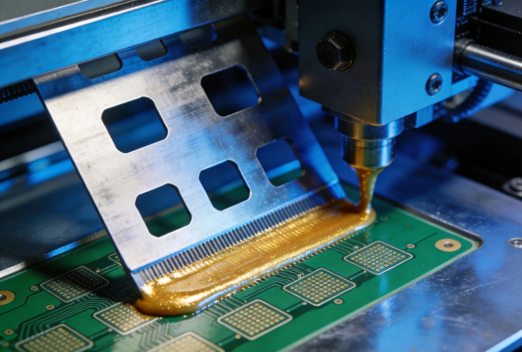
The stencil is a thin metal sheet—typically stainless steel or nickel—with apertures laser-cut, chemically etched, or electroformed to match the PCB pad pattern. The stencil sits on top of the PCB, and solder paste is forced through the apertures by the squeegee to deposit paste onto the pads below.
Stencil thickness is one of the most critical parameters in solder paste printing. It is measured in mils (thousandths of an inch) or micrometers. Common thicknesses range from 3 mils (75 micrometers) for fine-pitch applications to 8-10 mils (200-250 micrometers) for larger components like BGAs or connectors.
The relationship between stencil aperture dimensions and deposit volume is described by the area ratio and aspect ratio:
When these ratios are too low, paste tends to stick inside the aperture rather than release onto the pad—a phenomenon known as paste incompletion or mid-chip voiding. As component packages shrink and pad sizes decrease, stencil design becomes increasingly challenging.
A complete solder paste printing cycle consists of several distinct phases, each governed by different physical mechanisms:
1. Stencil alignment and separation: The stencil is aligned to the PCB using vision systems and fiducial markers. After printing, the stencil separates from the board. The separation speed and angle (called the peel rate or separation speed) critically affect paste release. A controlled, gradual separation allows the paste to stretch and release cleanly from the aperture walls. Too fast a separation causes the paste to collapse or bridge.
2. Squeegee action: The squeegee blade travels across the stencil, forcing paste into the apertures and across the surface. Squeegee pressure, speed, angle, and material all influence how effectively paste fills the apertures and cleans the stencil surface between prints.
3. Paste rolling: As the squeegee moves, solder paste forms a rolling ball in front of the blade. This rolling action helps keep the solder powder uniformly distributed and prevents the flux from separating from the powder. Adequate paste volume in front of the squeegee is necessary for proper rolling.
4. Aperture filling: The paste fills the stencil apertures through a combination of pressure from the squeegee and the viscous flow properties of the paste. The fill rate depends on paste rheology, aperture geometry, and squeegee parameters.
5. Paste release: During stencil separation, paste releases from the aperture walls onto the PCB pad. Release is affected by surface energies at the paste-stencil and paste-pad interfaces, aperture geometry, and the rheological recovery of the paste.
The interaction between solder paste, the stencil surface, and the PCB pad surface is governed by surface energy—the energy at the interface between different materials. Surface energy determines whether paste spreads, adheres, or releases.
A PCB pad with high surface energy (hydrophilic) attracts solder paste and promotes good spreading and adhesion. A pad with low surface energy (hydrophobic) repels paste and causes poor wetting and inconsistent deposits. Surface energy is affected by pad material, surface finish (HASL, ENIG, OSP, etc.), and cleanliness.
Stencil surface treatments—such as electropolishing to smooth the aperture walls, nano-coatings to reduce surface energy, or roughening to increase it—can dramatically affect paste release. Electropolished stainless steel stencils have smooth walls that reduce paste adhesion, while nanocoated stencils create low-surface-energy environments that promote clean release.
The solder paste printing process involves many interrelated parameters. Optimizing these parameters requires understanding how each one affects print quality and how they interact with each other.
Squeegee pressure must be sufficient to push paste through apertures and clean the stencil surface without being so high that it causes paste to squeeze out from under the blade and onto the board surface (causing smear or bridging). Typical pressure ranges from 0.2-0.4 kg per centimeter of squeegee length.
Squeegee speed affects the shear rate applied to the paste. Slower speeds (25-50 mm/s) allow better paste filling for fine-pitch applications but reduce throughput. Faster speeds (75-150 mm/s) increase throughput but may compromise fill on very fine features. Most manufacturers use speeds of 25-75 mm/s as a starting point.
Squeegee material and geometry also matter. Metal squeegee blades provide consistent pressure and are preferred for fine-pitch applications. Rubber squeegees are less expensive but wear faster and provide less consistent pressure. Squeegee angle (typically 45-75 degrees from horizontal) affects how paste is pushed and how much pressure is applied.
Dual-squeegee systems—using one squeegee for forward stroke and another for return stroke—can improve consistency and reduce setup time. Some modern printers use closed-loop pressure control to maintain constant squeegee force throughout the print cycle.
Proper board support is critical for achieving consistent print results. A PCB that lifts or bows during printing creates gaps between the stencil and pad, causing inconsistent paste deposits. The best results come from:
The clamping force must be sufficient to hold the board firmly without deforming it. Too little clamping causes board movement during printing; too much can stress or damage the board.
The snap-off distance is the gap between the stencil and the PCB after the printing stroke but before separation. A small snap-off distance (0-0.5 mm) provides the most consistent results for fine-pitch printing because it minimizes the distance the paste must stretch during separation. Larger snap-off distances may be used for larger apertures but can cause paste stretching, slumping, or incomplete release.
Separation speed controls how quickly the stencil peels away from the PCB after printing. A slower separation speed (0.5-2.0 mm/s) generally produces better paste release because it allows the paste to stretch and release gradually from the aperture walls. Some printers use a two-stage separation with a slow initial peel followed by faster retraction.
Environmental conditions significantly affect solder paste behavior. The ideal printing environment is:
Most manufacturers store solder paste refrigerated (typically 0-10°C) to extend shelf life. Paste should be allowed to thaw to room temperature before use—typically 2-4 hours depending on the package size. Using paste that is not fully thawed causes inconsistent viscosity and poor printing performance.
Stencil cleaning is essential for maintaining print quality, especially for fine-pitch applications. Between prints, a small amount of paste residue can accumulate on the bottom of the stencil, causing incomplete paste release and bridging defects.
Dry wiping (using a dry or slightly damp wipe) removes bulk paste from the stencil surface but may not clean aperture walls effectively.
Wet wiping with appropriate stencil cleaning solvents dissolves flux residues and provides more thorough cleaning. Automatic stencil cleaners use combinations of brushes, spray jets, and vacuum to clean both sides of the stencil between prints.
The cleaning frequency depends on the board design, paste type, and quality requirements. Fine-pitch boards (0.4 mm pitch and below) may require cleaning every 1-5 prints, while larger pad sizes may tolerate 10-20 prints between cleaning cycles.
Stencil design and manufacturing have advanced significantly in recent years, providing new options for improving paste release and print quality.
Laser-cut stencils are the most common type for SMT applications. A CO2 or fiber laser cuts apertures through the stainless steel sheet, producing clean, precise edges. The laser cutting process creates a slight taper (wider at the bottom than the top) that generally promotes good paste release.
Laser-cut stencils offer excellent dimensional accuracy, fast turnaround (often same-day for standard designs), and compatibility with a wide range of aperture sizes. They are suitable for most SMT applications including fine-pitch components down to 0.3 mm pitch.
Electropolishing is a post-processing treatment that removes material from the stencil surface using electrochemical action. It smooths the aperture walls, reducing surface roughness and creating a low-energy surface that promotes paste release.
Electropolished stencils are particularly beneficial for:
Nanocoating applies a ultra-thin polymer layer (typically 1-5 nanometers) to the stencil surface. This coating creates a low-surface-energy environment that dramatically reduces paste adhesion to the stencil walls and surface.
Nanocoated stencils can significantly reduce bridging and solder theft defects, especially for challenging aperture geometries. However, the coating wears off over time with repeated cleaning cycles and may need to be reapplied.
Electroformed stencils are created by plating nickel onto a mandrel in the shape of the desired apertures. This process produces stencils with very smooth walls and near-vertical sidewalls, offering excellent paste release characteristics.
Electroformed stencils are typically more expensive than laser-cut stencils but provide superior performance for the most demanding fine-pitch applications. They are commonly used for:
Step stencils use varying thickness in different areas of the same stencil. Thicker sections deposit more paste where needed (such as for large BGAs or connectors), while thinner sections provide fine-pitch capability where component density is highest.
Step stencils are created by:
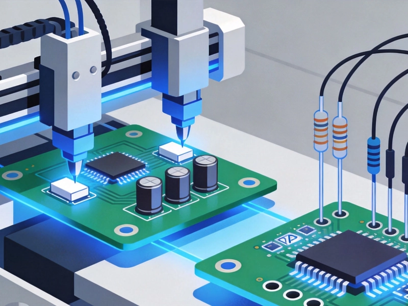
Modern SMT assembly relies heavily on automated inspection to catch defects before they propagate through the assembly process. Solder paste inspection (SPI) is the first line of defense.
SPI systems use 3D measurement technology—typically laser profilometry or structured light projection—to measure the height, area, and volume of printed solder paste deposits immediately after printing. This provides quantitative data for process control and defect detection.
Key measurements include:
SPI systems can be configured with defect classifications based on the criticality of the component and the process capability. Critical components (fine-pitch ICs, BGAs) may have tight tolerances, while larger passive components may tolerate greater variation.
Effective SPI requires setting appropriate thresholds for pass/fail criteria. Too tight a threshold causes excessive false rejects (good boards flagged as defective), reducing yield. Too loose a threshold allows defective boards to pass, causing downstream defects and field failures.
Statistical process control (SPC) techniques help establish appropriate thresholds based on actual process capability. Key metrics include:
Advanced SPI systems can provide closed-loop feedback to the printer, automatically adjusting parameters to correct for process drift. This might include:
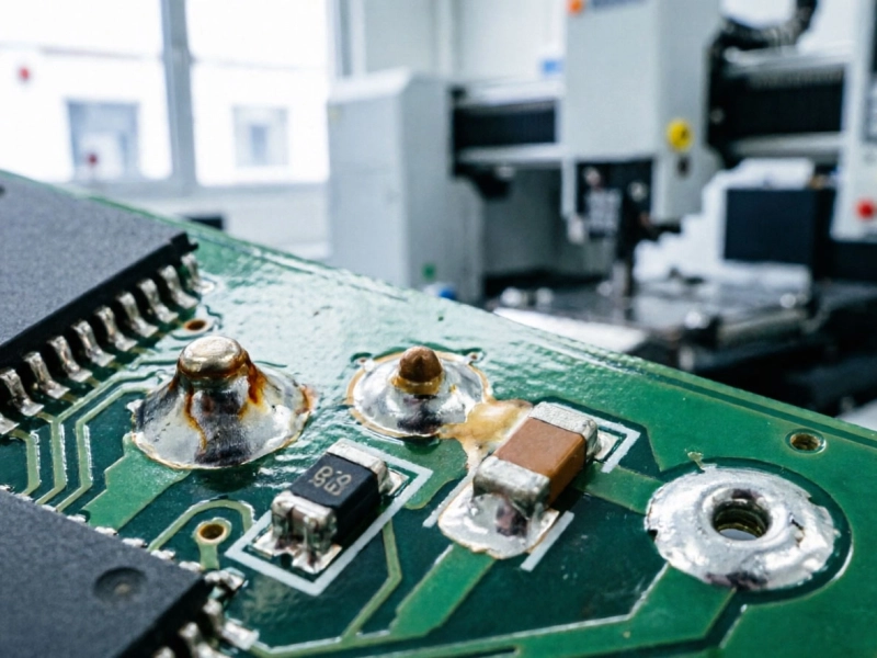
Understanding common solder paste printing defects and their root causes is essential for effective troubleshooting and process optimization.
| Defect | Symptom | Primary Root Causes | Solutions |
|---|---|---|---|
| Insufficient paste / Low volume | Deposit smaller than expected; missing paste areas | Low stencil thickness, aperture clogging, low squeegee pressure, high squeegee speed, poor paste flow, worn stencil | Increase thickness, improve cleaning, adjust pressure/speed, check paste viscosity, replace stencil |
| Excess paste / High volume | Deposit larger than expected; paste spreading beyond pad | Too much stencil thickness, aperture too large, low squeegee pressure (paste not cleaned), low viscosity paste | Reduce thickness, verify aperture size, increase pressure, use higher viscosity paste |
| Bridge / Short | Paste connecting adjacent pads | Too much paste, smear from squeegee, poor aperture design, paste slump, contamination between pads | Reduce paste volume, increase cleaning, improve aperture design, adjust snap-off, clean board surface |
| Incomplete release / Paste sticking | Paste remaining in stencil apertures after separation | Low area ratio, rough aperture walls, high surface energy stencil, improper separation speed, contaminated paste | Improve aspect/area ratio, electropolish or coat stencil, slow separation speed, check paste shelf life |
| Scrolling / Trailing | Paste stretching and trailing behind deposit during separation | Too slow separation, high viscosity paste, wide aperture walls, bottom stencil contamination | Increase separation speed, use lower viscosity paste, improve stencil design |
| Smear | Paste spread across board surface outside pads | Too much squeegee pressure, worn or damaged squeegee blade, excessive paste volume, low stencil contact | Reduce pressure, replace blade, reduce paste volume, improve board support |
| Offset / Misregistration | Paste deposit not aligned with pad | Misaligned stencil, PCB not properly clamped, fiducial recognition error, board warpage | Realign stencil, improve clamping, check vision system, verify board flatness |
| Paste slump | Paste spreading after printing, losing shape | High temperature, high humidity, low viscosity paste, paste agitated too much | Control environment, use slump-resistant paste, minimize paste handling before printing |
| Voiding (pre-reflow) | Bubbles or gaps visible in paste deposit | Contaminated paste, moisture in paste, aged paste, excessive mixing or stirring | Use fresh paste, store properly, minimize agitation, check paste lot date |
Based on the science and engineering principles discussed above, here are proven best practices for achieving and maintaining excellent solder paste printing results.
Before optimizing, establish a known-good baseline using Design of Experiments (DOE). Test different combinations of key parameters (pressure, speed, snap-off distance, separation speed) to understand their effects and identify the optimal operating window. Document results and use statistical analysis to determine the optimal settings.
Temperature and humidity variations directly affect paste viscosity and print consistency. Maintain tight control of the assembly environment (20-25°C, 30-60% RH). Monitor conditions continuously and alert operators when parameters drift outside limits. Consider using in-line environmental monitoring that correlates data with SPI measurements.
Follow manufacturer guidelines for paste storage, thawing, and usage. Track paste lot numbers and expiration dates. Do not use paste beyond its recommended working life on the stencil (typically 8-24 hours depending on conditions). Avoid excessive agitation or stirring that can cause the powder and flux to separate. Rotate stock using FIFO (first in, first out) inventory management.
Use SPI data not just for pass/fail screening but for statistical process control. Track trends over time to detect process drift before it causes defects. Monitor key parameters like deposit volume Cpk and defect rates. Use control charts to set realistic alarms and alerts.
No single stencil design works optimally for all boards. Analyze the board's component mix, pad sizes, and quality requirements to select the appropriate stencil technology and parameters. For boards with mixed fine-pitch and large-pitch components, consider step stencils or multiple print programs with different stencils.
Establish preventive maintenance schedules for printers, squeegees, and stencil cleaning equipment. Replace worn squeegee blades regularly (typically every 8 hours of operation or daily). Inspect stencils for damage, wear, and contamination. Clean and calibrate vision systems for accurate alignment.
Even with advanced automation, human operators play a critical role in solder paste printing. Ensure operators understand the science behind the process, not just the procedures. Train them to recognize early warning signs of process issues and respond appropriately. Encourage a culture of continuous improvement where operators feel empowered to suggest and implement improvements.
Solder paste printing technology continues to evolve to meet the demands of ever-shrinking electronics and increasing quality requirements.
As component packages continue to shrink—0.3 mm pitch, 0.2 mm pitch, and beyond—solder paste printing faces increasing challenges. New powder technologies (Type 6 and finer), advanced stencil materials (nanostructured coatings), and precision printing equipment are being developed to address these requirements.
Smart factories are integrating solder paste printing with broader manufacturing execution systems (MES). Real-time data collection, machine learning algorithms, and predictive analytics are being used to anticipate process issues before they occur, rather than reacting to defects after the fact.
Environmental concerns are driving innovation in solder paste formulation and cleaning processes. Water-based stencil cleaning systems, halogen-free fluxes, and lead-free alloys that reduce reflow temperatures (and thus energy consumption) are becoming more prevalent.
Typical squeegee pressure ranges from 0.2-0.4 kg per centimeter of squeegee length. However, the ideal pressure depends on your specific board design, paste type, and printer. The goal is to achieve complete paste filling without causing paste smear or blade damage. Start with manufacturer recommendations and fine-tune based on inspection results.
Cleaning frequency depends on the board design and quality requirements. For fine-pitch boards (0.4 mm pitch and below), clean every 1-5 boards. For larger pitch boards, 10-20 boards between cleaning may be acceptable. Monitor SPI data to determine the optimal cleaning interval for your specific process.
Aperture clogging is typically caused by dried or degraded paste, inadequate paste viscosity, or poor paste flow from the cartridge. Ensure paste is stored and handled properly, use paste at recommended temperature, and check that the cartridge design allows adequate paste flow to the stencil.
Laser-cut stencils are cut using a laser beam and have slightly tapered walls. They offer good quality, fast turnaround, and reasonable cost. Electroformed stencils are plated with nickel and have straight, smooth walls. They provide superior paste release for the finest-pitch applications but are more expensive and have longer lead times.
Temperature significantly affects solder paste viscosity. At higher temperatures, paste becomes thinner (lower viscosity), which can cause slump and bridging. At lower temperatures, paste becomes thicker, leading to poor aperture fill and low deposit volumes. Maintain consistent temperature (20-25°C) in the assembly area for optimal results.
Bridges are typically caused by too much paste, paste smear from the squeegee, or paste slump after printing. Check that deposit volumes are within specification, squeegee blades are in good condition, cleaning is adequate, and environmental conditions (temperature, humidity) are controlled.
Most manufacturers recommend not using paste that has been on the stencil for more than 8-24 hours, depending on conditions. Extended exposure to air causes the flux to oxidize and dry, degrading paste performance. If you need to pause production, cover the stencil with a lid or seal it in a bag with a small amount of solvent-saturated wipe to maintain humidity.
Area ratio is the ratio of the aperture opening area to the aperture wall area. It predicts how well paste will release from the stencil onto the PCB. An area ratio of at least 0.66 is generally recommended. Low area ratio (small, deep apertures) tends to cause paste to stick in the stencil rather than release onto the pad.
Solder paste printing is both a science and an art. The science provides the fundamental understanding of metallurgy, fluid dynamics, surface chemistry, and precision engineering that governs the process. The art lies in applying this knowledge to real-world situations—balancing competing requirements, troubleshooting complex defects, and optimizing processes for specific products and production environments.
The key to success in solder paste printing is understanding that every parameter affects every other parameter. Viscosity influences pressure and speed. Temperature affects viscosity. Stencil design determines what is achievable with any given parameter set. By mastering the fundamentals outlined in this guide, you will be better equipped to diagnose problems, optimize your process, and achieve the consistent, high-quality results that modern electronics assembly demands.
Remember: approximately two-thirds of SMT defects originate from the printing stage. Investing in your solder paste printing process—in equipment, in training, in process control—delivers the highest return in overall assembly quality and yield. The science is well understood. The challenge lies in applying it consistently, day after day, board after board.

The Rise of AI in SMT Quality InspectionJune/18/2026
SMT vs. THT: Understanding the Differences in PCB Assembly TechnologiesMay/19/2026
Common SMT Defects and How to Prevent Them in Your DesignJuly/03/2026

Reflow Soldering Profiles Explained: Avoiding Thermal DefectsJuly/01/2026

Low Volume PCB Assembly for Startups The Ultimate GuideJune/03/2026