Open Nav


In the highly automated world of Surface Mount Technology (SMT), solder paste printing is universally recognized as the most critical step. Often referred to as the "first line of defense," this process dictates the volume, shape, and placement accuracy of the solder deposits. Industry data consistently shows that a vast majority of SMT defects can be traced back to the printing stage. Achieving perfect SMT assembly requires a deep understanding of the physics, material science, and mechanical precision that govern this process.
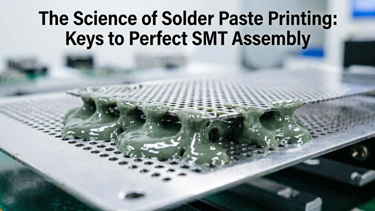
Solder paste is not a simple liquid; it is a complex, highly thixotropic suspension consisting of 88% to 90% metal alloy powder and 10% to 12% flux by weight. Its behavior changes dynamically under stress. During printing, the mechanical force of the squeegee shears the paste, temporarily lowering its viscosity so it can easily roll into and fill the stencil apertures. Once the squeegee passes and the shear force is removed, the paste must immediately recover its viscosity to hold its shape on the PCB pad.
If the paste lacks this thixotropic recovery, it will suffer from "cold slumping" at room temperature, leading to solder bridges. Conversely, if it is too stiff, it will not fill fine-pitch apertures, resulting in insufficient solder. Furthermore, as the board enters the reflow oven, the flux becomes highly fluid. If the preheat ramp rate is too slow, the paste can undergo "hot slumping" before the solder melts, again causing shorts.
The stencil acts as the precision mold for the solder paste. The most vital scientific metric in stencil design is the Area Ratio (AR), defined as the area of the aperture opening divided by the total area of the aperture sidewalls. According to IPC-7525 standards, an Area Ratio of at least 0.66 is required to ensure reliable paste release. If the AR falls below this threshold, surface tension and sidewall friction will cause the paste to stick inside the aperture rather than transferring cleanly to the pad.
Manufacturing technology also plays a massive role. While laser-cut stainless steel stencils are the industry standard, electroformed nickel stencils provide mirror-smooth sidewalls that drastically reduce friction, making them ideal for ultra-fine-pitch components like 01005 packages or micro-BGAs. Additionally, applying nano-coatings to the stencil can lower the surface energy, allowing paste to release cleanly even when geometric ratios are challenging.
Even with perfect paste and an optimal stencil, the mechanical execution must be flawless. Three primary parameters dictate the quality of the deposit:
In modern high-reliability manufacturing, printing must be immediately followed by Solder Paste Inspection (SPI). Using 3D optical systems, SPI machines measure the volume, height, area, and alignment of every single deposit with extreme precision. By catching defects like insufficient volume, bridging, or misalignment immediately after printing, manufacturers can prevent defective boards from moving to the pick-and-place and reflow stages, saving massive amounts of time and money on rework.
Perfect SMT assembly is not an accident; it is the result of mastering the science of solder paste printing. By respecting the rheological properties of the materials, adhering to strict geometric design rules like the Area Ratio, and meticulously tuning mechanical parameters, engineers can achieve near-perfect transfer efficiency. In the miniaturized era of modern electronics, controlling the printing process is the ultimate key to manufacturing reliable, high-quality circuit boards.

Sustainability in PCB Assembly: Green Manufacturing Practices for the Electronics IndustryJuly/10/2026
Low Volume PCB Assembly for Startups The Ultimate GuideJune/03/2026
SMT vs. THT: Understanding the Differences in PCB Assembly TechnologiesMay/19/2026
Offshore vs. Domestic PCB Assembly Services: Analyzing the Trade-offsJuly/16/2026

High-Reliability PCB Assembly Services for Automotive ElectronicsJuly/08/2026