Open Nav



The electronics industry faces an unprecedented challenge: meeting the world's insatiable demand for technology while minimizing environmental impact. PCB assembly, a cornerstone of modern electronics manufacturing, has traditionally been resource-intensive and environmentally challenging. However, a transformation is underway. Green manufacturing practices are reshaping how printed circuit boards are designed, produced, and disposed of, creating a more sustainable future for the electronics industry and the planet.
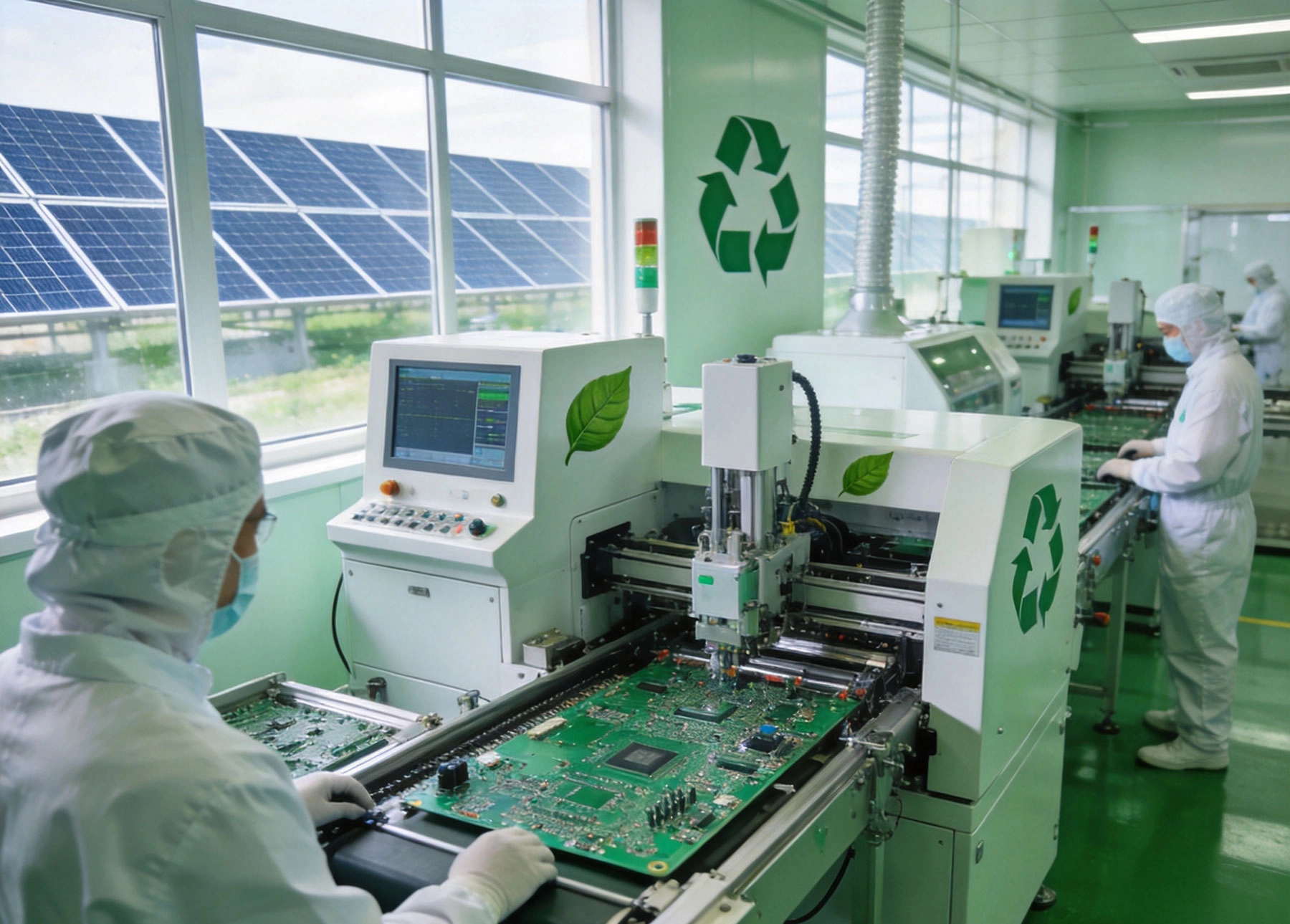
Understanding the environmental footprint of conventional PCB assembly is essential for appreciating the importance of sustainable practices. The electronics manufacturing process generates significant environmental burdens at every stage.
Traditional PCB manufacturing consumes vast amounts of raw materials including copper, gold, silver, and various chemical compounds. The production process generates substantial waste, from etching solutions and plating baths to rejected boards and packaging materials. A typical PCB Fabrication facility can produce hundreds of tons of hazardous waste annually, including heavy metals, acids, and organic solvents that require careful handling and disposal.
Water consumption presents another major concern. PCB manufacturing requires extensive water for cleaning, etching, and rinsing operations. A single manufacturing line can use thousands of liters of water daily, much of which becomes contaminated and requires treatment before discharge or reuse.
PCB assembly operations are energy-intensive. Soldering equipment, cleanroom HVAC systems, automated assembly lines, and testing equipment consume substantial electricity. Facilities operating 24/7 can accumulate massive energy bills and carbon emissions. The carbon footprint extends beyond direct manufacturing to include raw material extraction, component transportation, and end-of-life disposal.
Traditional PCB manufacturing involves numerous hazardous chemicals including lead-based solders, brominated flame retardants, volatile organic compounds, and strong acids. These substances pose risks to worker health and can contaminate air, water, and soil if not properly managed. The industry's historical reliance on lead solder, in particular, created significant environmental and health concerns that drove regulatory changes worldwide.
The transition to sustainable PCB assembly begins with material selection. Green materials reduce environmental impact throughout the product lifecycle while maintaining performance and reliability.
The shift from lead-tin solder to lead-free alternatives represents one of the most significant environmental improvements in PCB assembly. The European Union's Restriction of Hazardous Substances (RoHS) directive, implemented in 2006, catalyzed global adoption of lead-free soldering. Common lead-free alloys include tin-silver-copper (SAC), tin-copper, and tin-silver compositions.
These alternative solders eliminate toxic lead from the manufacturing process and end products, reducing health risks for workers and environmental contamination. While lead-free soldering initially presented technical challenges including higher processing temperatures and different wetting characteristics, process optimization and improved alloy formulations have largely addressed these concerns.
Traditional PCB substrates incorporate brominated flame retardants to meet fire safety requirements. However, these halogenated compounds can release toxic dioxins and furans when burned or improperly disposed. Halogen-free alternatives use phosphorus-based or nitrogen-based flame retardants that provide equivalent fire protection with reduced environmental impact.
Major substrate manufacturers now offer comprehensive lines of halogen-free materials suitable for various applications from consumer electronics to high-reliability aerospace systems. These materials meet stringent flammability standards while supporting sustainability goals.
Emerging technologies promise even more sustainable substrate options. Researchers are developing biodegradable PCB materials using natural fibers, biopolymers, and organic compounds. While not yet suitable for all applications, these materials offer exciting possibilities for reducing electronic waste.
Recyclable substrate designs facilitate material recovery at end-of-life. Some innovative approaches use reversible adhesives and separable material layers that enable efficient component and material reclamation during recycling processes.
Surface finish selection significantly impacts environmental footprint. Traditional hot air solder leveling (HASL) uses lead-containing solders and generates fumes requiring extensive ventilation and treatment. Alternative finishes offer greener solutions:
Electroless Nickel Immersion Gold (ENIG): Provides excellent solderability and shelf life without lead. The process uses less hazardous chemicals and generates less waste than traditional alternatives.
Organic Solderability Preservatives (OSP): Use organic compounds to protect copper surfaces. This water-based process eliminates heavy metals and reduces chemical usage.
Immersion Tin and Silver: Offer lead-free alternatives with good solderability and compatibility with various assembly processes.
Reducing energy consumption is crucial for sustainable PCB assembly. Manufacturing facilities are implementing comprehensive energy management strategies that cut costs while minimizing environmental impact.
Leading PCB manufacturers are investing in renewable energy sources to power their operations. Solar panel installations on factory rooftops, power purchase agreements with wind farms, and on-site renewable generation reduce dependence on fossil fuels. Some facilities achieve significant portions of their energy needs from renewable sources, dramatically reducing their carbon footprint.
Energy storage systems complement renewable generation, storing excess solar or wind power for use during peak demand periods. This approach maximizes renewable energy utilization while reducing electricity costs and grid dependence.
Modern assembly equipment incorporates energy-saving features including intelligent power management, variable speed drives, and optimized heating systems. Reflow ovens with advanced thermal profiling reduce energy consumption while maintaining process quality. LED lighting replaces traditional fixtures throughout facilities, cutting lighting energy use by 50% or more.
Process optimization further reduces energy requirements. Improved thermal profiles minimize heating and cooling cycles. Optimized production scheduling maximizes equipment utilization and reduces idle time. These operational improvements compound the benefits of efficient equipment.
Advanced building management systems control HVAC, lighting, and equipment based on actual needs rather than fixed schedules. Occupancy sensors, temperature monitoring, and automated controls ensure energy is used only when and where needed. Cleanroom facilities, traditionally major energy consumers, benefit significantly from optimized air handling and filtration systems.
Sustainable PCB assembly embraces circular economy principles, minimizing waste generation and maximizing material recovery. This approach transforms waste from a disposal problem into a resource opportunity.
Recycling begins at the design stage. Design for recycling (DfR) principles ensure products can be efficiently disassembled and materials recovered at end-of-life. Key considerations include:
Material Selection: Choosing materials compatible with existing recycling processes and avoiding hazardous substances that complicate material recovery.
Component Accessibility: Designing products that can be easily disassembled to separate valuable components and materials.
Material Identification: Marking plastic components with appropriate recycling codes to facilitate sorting and processing.
Unified Material Sets: Minimizing the variety of materials used in a product to simplify recycling and improve material purity.
Lean manufacturing principles reduce waste generation during production. Just-in-time component delivery minimizes packaging waste and inventory obsolescence. Optimized panelization maximizes material utilization and reduces scrap. First-article inspection and process control reduce defect rates, decreasing rework and scrap generation.
Water conservation programs significantly reduce consumption and wastewater generation. Closed-loop water systems recycle process water, treating it for reuse rather than discharge. Advanced filtration and purification technologies enable water recycling without compromising process quality.
Process chemicals represent both environmental and economic concerns. Modern facilities implement chemical recovery systems that regenerate and reuse process solutions. Etching solutions, plating baths, and cleaning chemicals can often be recycled multiple times before requiring disposal or regeneration.
On-site chemical recycling reduces purchase costs, waste generation, and disposal expenses. For chemicals that cannot be recycled internally, specialized waste management companies recover valuable materials and treat residual waste appropriately.
Packaging waste represents a significant environmental impact for electronics manufacturing. Sustainable packaging initiatives include:
Minimal Packaging: Right-sizing packaging to product dimensions reduces material usage and transportation impacts.
Recycled Content: Using packaging materials with high recycled content, including post-consumer recycled plastics and paper.
Biodegradable Alternatives: Replacing traditional plastics with biodegradable or compostable materials where appropriate.
Reusable Packaging Systems: Implementing returnable packaging for component delivery and product shipment.
Water management is critical for sustainable PCB manufacturing. Facilities are implementing comprehensive programs to reduce consumption, recycle process water, and ensure discharged water meets stringent environmental standards.
Advanced water treatment systems enable extensive recycling of process water. Membrane filtration, reverse osmosis, and ion exchange remove contaminants, producing water suitable for reuse in manufacturing processes. Some facilities achieve water recycling rates exceeding 80%, dramatically reducing freshwater consumption and wastewater discharge.
Zero-liquid discharge systems represent the ultimate goal, completely eliminating wastewater discharge through comprehensive recycling and evaporation technologies. While capital-intensive, these systems eliminate regulatory compliance concerns and water supply risks.
Modern wastewater treatment systems remove heavy metals, organic compounds, and other contaminants before discharge. Chemical precipitation, electrocoagulation, and advanced oxidation processes ensure treated water meets or exceeds regulatory requirements. Some facilities recover valuable metals from wastewater, transforming waste treatment from a cost center into a revenue source.
Sustainable PCB assembly extends beyond the manufacturing facility to encompass the entire supply chain. Responsible sourcing, supplier collaboration, and logistics optimization contribute to comprehensive sustainability programs.
Electronics manufacturing relies on minerals including tin, tantalum, tungsten, and gold. Irresponsible mining of these materials has funded conflict and human rights abuses in certain regions. Regulatory requirements including the Dodd-Frank Act in the United States and the EU Conflict Minerals Regulation require companies to trace mineral sources and ensure responsible sourcing.
Sustainable PCB manufacturers implement rigorous due diligence programs, working with certified smelters and refiners to ensure supply chain integrity. Blockchain and other traceability technologies provide increasing transparency into material origins.
Leading manufacturers extend sustainability requirements to their suppliers. Environmental audits, sustainability scorecards, and collaborative improvement programs help suppliers reduce their environmental impact. This approach multiplies the environmental benefits throughout the supply chain.
Transportation emissions represent a significant portion of electronics manufacturing's carbon footprint. Optimization strategies include:
Consolidated Shipping: Combining shipments to maximize transportation efficiency and reduce per-unit emissions.
Modal Optimization: Selecting transportation modes based on distance, urgency, and environmental impact. Ocean freight and rail transport generally offer lower carbon intensity than air freight for appropriate shipments.
Local Sourcing: Sourcing components and materials from regional suppliers when possible to reduce transportation distances.
Packaging Optimization: Designing packaging for maximum density and protection, reducing both material usage and transportation requirements.
Climate change concerns are driving comprehensive carbon reduction programs across the electronics industry. PCB manufacturers are measuring, reporting, and reducing their greenhouse gas emissions through various strategies.
Accurate carbon accounting enables effective reduction strategies. Manufacturers track emissions across three scopes: direct emissions from owned sources (Scope 1), indirect emissions from purchased energy (Scope 2), and other indirect emissions including supply chain and product use (Scope 3). This comprehensive approach identifies the largest emission sources and prioritizes reduction efforts.
Manufacturing process improvements reduce both energy consumption and process emissions. Optimized thermal profiles in reflow ovens reduce natural gas consumption. Improved cleanroom efficiency cuts HVAC energy requirements. These operational improvements provide immediate emission reductions while often reducing operating costs.
While reduction remains the priority, some emissions are currently unavoidable. Carbon offset programs invest in verified emission reduction projects including reforestation, renewable energy, and methane capture. Some manufacturers are exploring carbon removal technologies that permanently sequester atmospheric carbon dioxide.
Sustainability in PCB assembly operates within an evolving regulatory framework. Compliance with environmental regulations is mandatory, but leading companies go beyond minimum requirements to achieve voluntary sustainability certifications.
RoHS (Restriction of Hazardous Substances): Limits hazardous substances in electrical and electronic equipment, including lead, mercury, cadmium, and hexavalent chromium.
WEEE (Waste Electrical and Electronic Equipment): Requires producers to take responsibility for end-of-life product collection, treatment, and recycling.
REACH (Registration, Evaluation, Authorization and Restriction of Chemicals): EU regulation addressing chemical substance safety throughout supply chains.
EPA Regulations: U.S. Environmental Protection Agency requirements for air emissions, wastewater discharge, and hazardous waste management.
Beyond regulatory compliance, manufacturers pursue voluntary certifications demonstrating environmental commitment:
ISO 14001: Environmental management system standard providing framework for environmental responsibility.
ISO 50001: Energy management system standard supporting energy efficiency improvements.
IPC-1752A: Materials declaration standard enabling supply chain transparency regarding material composition.
Carbon Disclosure Project (CDP): Global disclosure system for environmental impacts including climate change.
Sustainability in PCB assembly is not merely an environmental imperative—it makes sound business sense. Green manufacturing practices deliver tangible benefits that improve competitiveness and profitability.
Energy efficiency, water conservation, and waste reduction directly reduce operating costs. Material recycling and chemical recovery reduce purchase expenses. These operational savings often offset or exceed the costs of sustainability investments.
Environmental performance increasingly influences purchasing decisions. Major electronics brands prioritize suppliers with strong sustainability credentials. Green manufacturing capabilities provide competitive advantage in markets where customers value environmental responsibility.
Sustainable practices reduce exposure to regulatory risks, resource scarcity, and supply chain disruptions. Companies with robust environmental management systems are better positioned to adapt to evolving regulations and market conditions.
Strong environmental performance enhances brand reputation and stakeholder relationships. Employees prefer working for environmentally responsible companies. Investors increasingly consider environmental, social, and governance (ESG) factors in investment decisions.
The sustainability transformation in PCB assembly continues to accelerate. Emerging technologies and evolving practices promise further environmental improvements.
New recycling technologies improve material recovery rates and purity. Hydrometallurgical processes recover precious metals with higher efficiency than traditional smelting. Automated disassembly systems using robotics and artificial intelligence increase recycling throughput and reduce costs.
Research into bio-based substrates and components continues to advance. Materials derived from agricultural waste, algae, and other renewable sources may eventually replace petroleum-based alternatives in certain applications.
Smart manufacturing technologies optimize resource utilization and reduce waste. Real-time monitoring and predictive maintenance maximize equipment efficiency. Digital twins enable process optimization without physical experimentation, reducing material and energy consumption during development.
Product-as-a-service and take-back programs align manufacturer incentives with product longevity and recyclability. These business models encourage design for durability and repair while ensuring responsible end-of-life management.
Sustainability in PCB assembly has evolved from a regulatory compliance challenge to a strategic business imperative. Green manufacturing practices deliver environmental benefits while improving operational efficiency, reducing costs, and enhancing competitiveness. The electronics industry is demonstrating that economic success and environmental responsibility can go hand in hand.
The transformation is far from complete. Emerging technologies promise further improvements in material sustainability, energy efficiency, and circular economy implementation. Companies that embrace this transformation will be best positioned to thrive in an increasingly sustainability-focused market.
For PCB manufacturers, the path forward is clear: invest in green materials, optimize energy and resource use, minimize waste generation, and collaborate with supply chain partners to extend sustainability throughout the value chain. The result is a more sustainable electronics industry that meets the world's technology needs while preserving the environment for future generations.
The primary concerns include hazardous waste generation (heavy metals, chemical solvents), high energy consumption, water pollution from manufacturing processes, use of toxic materials like lead and halogenated flame retardants, and end-of-life disposal challenges for electronic waste.
Lead-free soldering eliminates toxic lead from manufacturing processes and end products, reducing health risks for workers and environmental contamination. It enables compliance with regulations like RoHS and supports circular economy goals by making products safer to recycle.
Design for Recycling incorporates end-of-life considerations into product design. This includes selecting recyclable materials, ensuring components can be easily separated, minimizing material variety, and avoiding hazardous substances that complicate recycling processes.
Strategies include transitioning to renewable energy, improving equipment energy efficiency, optimizing logistics and transportation, reducing material waste, implementing process improvements, and investing in carbon offset programs for unavoidable emissions.
Key certifications include ISO 14001 (environmental management), ISO 50001 (energy management), RoHS compliance (hazardous substance restriction), and participation in the Carbon Disclosure Project. These demonstrate systematic approaches to environmental responsibility.
Streamlining Production with Integrated PCB Fabrication and AssemblyJuly/20/2026
Industrial Control Boards: Heavy Copper and Robust Assembly TechniquesSeptember/29/2026
The Evolution of Surface Mount Technology (SMT) in ElectronicsSeptember/20/2026
The Future of Flexible Hybrid Electronics (FHE) in AssemblyAugust/06/2026
Inventory Management Benefits of Using a Turnkey Assembly PartnerAugust/03/2026