Open Nav



Every PCB assembly decision eventually runs into the same fork in the road: leaded or lead-free solder? For decades, tin-lead alloys were the default choice in electronics manufacturing — reliable, well-understood, and easy to work with. Then environmental regulations changed the equation. The European Union's Restriction of Hazardous Substances (RoHS) directive, first introduced in 2006 and expanded since, pushed most consumer electronics toward lead-free alternatives. Today, most of the world's contract manufacturers default to lead-free processes, but leaded solder has not disappeared — it persists in aerospace, automotive, defense, and medical sectors where reliability trumps regulatory preference.
The choice between the two is not as simple as "green versus traditional." Each alloy family brings distinct advantages, real tradeoffs, and manufacturing implications that affect everything from reflow profile design to long-term field reliability. Understanding those differences matters whether you are specifying a new product, qualifying a contract manufacturer, or debugging a recurring solder joint failure.
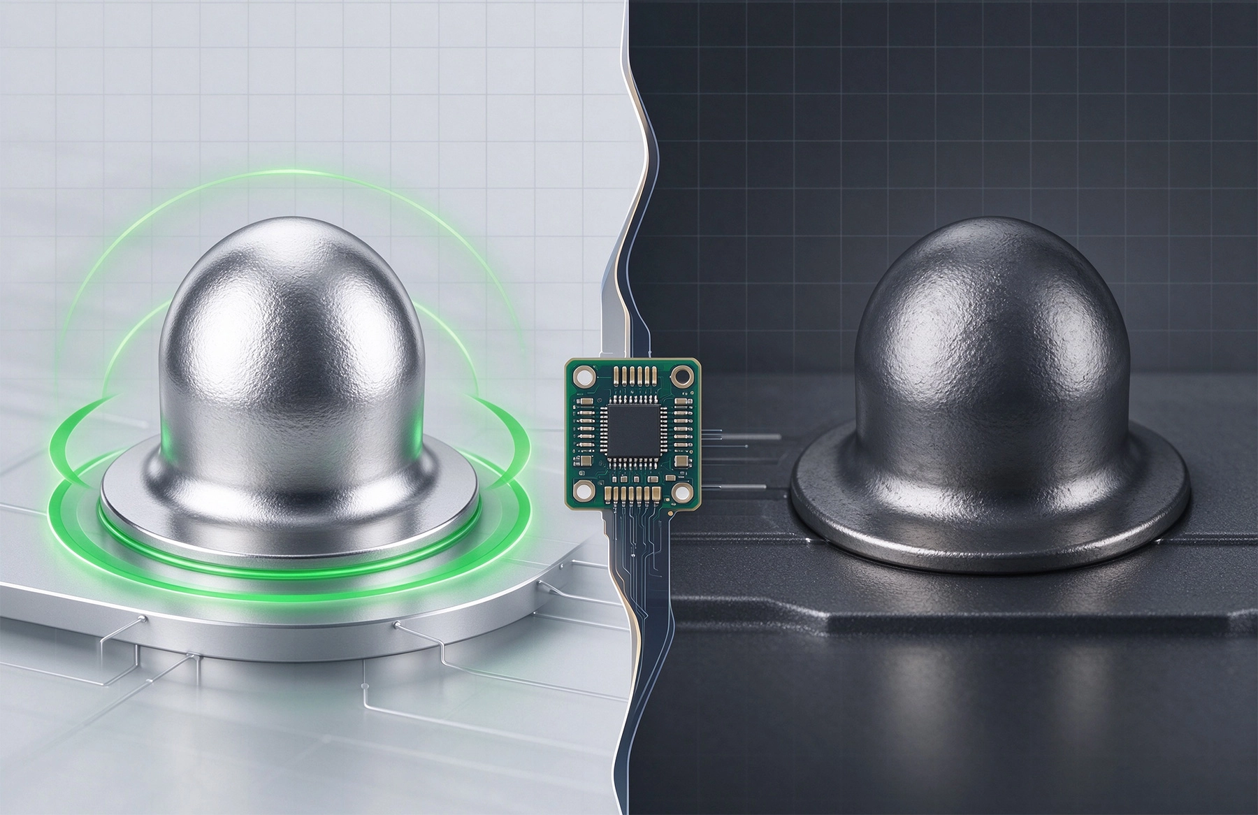
Traditional leaded solder for electronics is almost always a tin-lead eutectic alloy — most commonly Sn63 (tin 63%, lead 37%) or Sn60/40. The eutectic composition melts at a single sharp point of 183 °C, which makes the reflow window predictable and forgiving. Leaded solder also wets copper surfaces readily, produces a smooth shiny joint, and tolerates slight variations in profile temperature without degrading quality.
Lead-free solders replace lead with other metals — typically silver, copper, bismuth, or antimony — to achieve a RoHS-compliant alloy. The most widely used lead-free composition is SAC305 (tin 96.5%, silver 3%, copper 0.5%), which melts in a range around 217–220 °C. Other variants like SnBi (tin-bismuth) or low-silver alloys offer lower melting points for temperature-sensitive assemblies, but SAC305 remains the industry workhorse for its balance of mechanical strength and wetting behavior.
The 183 °C melting point of Sn63 is roughly 35 °C lower than SAC305. That difference matters in production. A lower peak temperature means less thermal stress on nearby components, laminates, and connectors that may not tolerate the higher heat exposure that lead-free demands. It also gives the reflow oven a wider process window: if the actual peak temperature drifts a few degrees above or below target, the joint quality is less likely to suffer.
Lead improves the flow characteristics of solder on copper pads. Leaded joints tend to form smooth, concave fillets with a bright, matte-satin finish that is visually reassuring. Wetting is faster and more complete, which reduces the risk of cold joints, non-wet opens, and other defects that plague assemblies with poor solderability. This is particularly valuable in hand-assembly and rework scenarios where a technician is working with a soldering iron rather than a reflow oven.
When a defect is found after reflow, repair technicians generally find leaded solder easier to work with. The lower melting point means less time applying heat to the joint, which reduces the risk of lifting pads, damaging nearby traces, or overheating temperature-sensitive components. Leaded solder also re-flows more readily when adding fresh solder to a repair joint, producing a reliable reconnection without the aggressive thermal exposure required by lead-free rework.
Aerospace, defense, and certain medical device manufacturers continue to specify leaded solder not because they are ignoring regulations — many hold RoHS exemptions under Annex III or operate under commercial-off-the-shelf (COTS) frameworks — but because the alloy's fatigue performance is well-characterized in thermal cycling environments. Sn63/Pb37 joints exhibit superior resistance to thermal fatigue crack propagation compared to some early lead-free formulations, and decades of field data back that performance record.
RoHS compliance is a hard requirement for most product categories sold in the EU, China, South Korea, and increasingly other jurisdictions. Consumer electronics, household appliances, IT equipment, and a wide range of industrial products cannot legally carry leaded solder if they want access to those markets. A design that uses leaded solder by default will require a separate, leaded-specific build for exempt applications — adding complexity to the supply chain and increasing per-unit cost.
Lead is a neurotoxin. While the exposure risk from a finished assembled board is negligible under normal use, occupational exposure during manufacturing, and improper disposal at end-of-life, creates legitimate environmental and health concerns. RoHS was designed precisely to eliminate that pathway. For companies with sustainability mandates or ESG reporting obligations, the environmental profile of leaded solder is difficult to defend regardless of its technical merit.
As lead-free has become the global default, the availability of leaded-solder-compatible components is narrowing. Some BGA packages, advanced connectors, and specialized ICs are now manufactured only with RoHS-compliant finishes. Building a leaded assembly with components whose terminations are already lead-free can create a metallurgical mismatch at the joint interface, potentially degrading reliability rather than improving it.
For the vast majority of electronics products, RoHS compliance is non-negotiable. Lead-free solder is the default path to accessing global markets without regulatory friction. It also positions a product favorably for WEEE (Waste Electrical and Electronic Equipment) recyclability certifications and circular economy compliance schemes that are gaining traction in EU and Asia-Pacific regulatory frameworks.
SAC305 and comparable lead-free alloys produce joints with higher tensile strength and better creep resistance than tin-lead eutectic. Under mechanical shock — the kind of drop-test and vibration environment common in handheld devices and automotive under-hood electronics — lead-free joints tend to resist cracking better. This strength advantage has improved steadily as lead-free formulations have matured over the past fifteen years of high-volume production experience.
The higher melting point of lead-free solder gives joints greater thermal stability at elevated operating temperatures. For products that must function in high-ambient-temperature environments — automotive engine compartments, industrial controls near process heat sources, LED lighting housings — the increased thermal margin of lead-free joints can extend service life. Leaded joints at sustained temperatures above 100 °C are more prone to creep and intermetallic growth that degrades joint integrity over time.
Gold-plated component terminations — common in connectors and some IC packages — can cause embrittlement in leaded solder when the gold dissolves into the joint and forms AuSn4 intermetallic compounds. Lead-free solders, particularly those with higher silver content, are generally more tolerant of gold dissolution, reducing the risk of brittle joint failures in assemblies with gold-finished components.
The ~35 °C higher melting point of SAC305 compared to Sn63 forces a higher peak reflow temperature — typically 245–260 °C versus 225–235 °C for leaded processes. This increased thermal load stresses the entire assembly: laminate materials see greater z-axis expansion, which raises the risk of barrel cracking in plated through-holes; nearby connectors and electromechanical switches may not survive the temperature exposure; and moisture-sensitive components require more rigorous dry-bake procedures before assembly to avoid delamination and pop-corning.
Lead-free solder is less fluid than tin-lead at equivalent temperatures, and it oxidizes more readily on the surface of the molten pool. This demands a more active flux chemistry — typically no-clean or water-soluble fluxes with higher activation levels — and tighter control over the reflow atmosphere. Nitrogen inerting in the reflow oven becomes more important for lead-free assemblies to achieve consistent wetting and avoid voids. Without proper process control, lead-free assemblies are more prone to poor fillet formation, icicle bridging, and non-wet opens.
Pure tin and high-tin lead-free alloys are susceptible to tin whisker growth — spontaneous metallic filament growth from the solder surface that can bridge adjacent conductors and cause short circuits. While tin whisker research has advanced considerably and mitigation strategies ( matte tin finishes, lead addition, conformal coating, underfill) are well established, the risk remains higher than with leaded solders, where lead suppresses whisker formation naturally. High-reliability applications with long service life requirements must account for this in the reliability model.
Lead-free rework is genuinely harder. The higher melting point means more heat must be applied for longer, which increases the risk of pad lift, trace delamination, and thermal damage to adjacent components. Technicians need more specialized equipment — hot-air rework stations with precise temperature and airflow control, high-quality soldering tips — and more training. The slower wetting also means it takes longer to achieve a reliable repair joint, and the visual appearance of lead-free repair joints is often less smooth and less reassuring than their leaded counterparts.
When some components in an assembly are lead-free and others are not — a situation that arises frequently in mixed-technology products — the manufacturer must manage a split BOM where some devices are RoHS-compliant and others are not. This complicates inventory control, introduces the risk of cross-contamination in the assembly line, and makes the supply chain harder to audit for compliance. For products that must maintain a single compliant BOM, lead-free is the only viable path regardless of other considerations.
Regardless of alloy choice, flux selection and residue management are critical. No-clean fluxes leave a thin residue that is generally acceptable for most applications but may interfere with conformal coating or high-voltage isolation. Water-soluble fluxes produce a cleaner appearance but require thorough washing and drying — any residue left behind on the board acts as a hygroscopic contaminant that accelerates corrosion under humidity. The choice of flux type should align with the end-product's operating environment and any applicable industry standards.
Both leaded and lead-free solder joints form intermetallic compound (IMC) layers at the copper-solder interface — typically Cu6Sn5 for tin-based solders, with Cu3Sn appearing as the joint ages. Excessive IMC growth, especially in high-temperature lead-free reflow cycles, can make the joint brittle. Controlling peak reflow temperature, dwell time above liquidus, and the number of reflow cycles keeps the IMC layer within acceptable thickness limits (generally below 2–3 microns for reliable joints).
Modern lead-free assemblies often contain moisture-sensitive components — BGAs, QFNs, and microprocessors — that require dry storage and controlled exposure times after dry-bake. Both leaded and lead-free assembly lines must observe strict ESD controls, but the higher thermal budgets of lead-free processing make thermal fatigue-induced failure modes more likely in components that are not properly handled before assembly.
For most commercial and consumer electronics, the decision is already made: lead-free is required for regulatory compliance and no alternative exists. For those products, the engineering effort shifts from alloy selection to process optimization — tuning the reflow profile, managing moisture sensitivity, and controlling rework quality to extract maximum reliability from the lead-free system.
For aerospace, defense, automotive safety-critical, and certain medical electronics, the choice is more nuanced. Leaded solder may be legally available under RoHS exemptions, but the supply chain for leaded-compatible components is shrinking, and the long-term availability of leaded processes is uncertain as manufacturers consolidate around lead-free as their default line. Teams in these sectors should be conducting active lifecycle assessments of their solder strategy and qualifying backup processes before a regulatory or supply-chain change forces their hand.
Neither leaded nor lead-free solder is universally superior. Leaded solder offers manufacturing friendliness, lower thermal stress, and decades of proven reliability data — but it is increasingly restricted by regulation and supply chain availability. Lead-free solder meets global compliance requirements and delivers stronger joints in mechanical shock environments — but it demands tighter process control, more sophisticated equipment, and more careful handling of moisture-sensitive components.
The most pragmatic approach is to treat the choice as a system-level decision, not just a metallurgy question. Evaluate the product's regulatory context, its operating environment, the expected service life, and the manufacturing capabilities available. Then build the assembly process around the alloy that best fits that complete picture — rather than defaulting to convention or convenience.
Contact us to discuss your requirements.
The Role of SPI (Solder Paste Inspection) in Reducing SMT DefectsSeptember/08/2026
High-Reliability PCB Assembly Services for Automotive ElectronicsJuly/08/2026
The Importance of Fiducial Marks and Tooling Holes in PCBAAugust/12/2026
Choosing the Right Surface Finish for Your SMT PCB AssemblySeptember/23/2026
Top 10 DFM (Design for Manufacturability) Tips for SMT PCB AssemblyJune/08/2026