Open Nav



In the world of modern electronics manufacturing, precision and accuracy are paramount. When it comes to PCB assembly (PCBA), even microscopic misalignments can lead to catastrophic failures, reduced product reliability, and costly rework. This is where fiducial marks and tooling holes play an indispensable role in ensuring the success of your printed circuit board assembly process. Understanding these critical design elements and implementing them correctly can mean the difference between a flawless assembly run and a production nightmare.
Fiducial marks and tooling holes serve as the navigation system for automated assembly equipment, providing precise reference points that guide component placement, solder paste printing, and inspection processes. Without these essential features, even the most sophisticated SMT assembly lines would struggle to achieve the level of accuracy required for today's high-density, miniaturized electronic devices. This comprehensive guide explores the importance of these features, their design requirements, and best practices for implementation in your PCB designs.
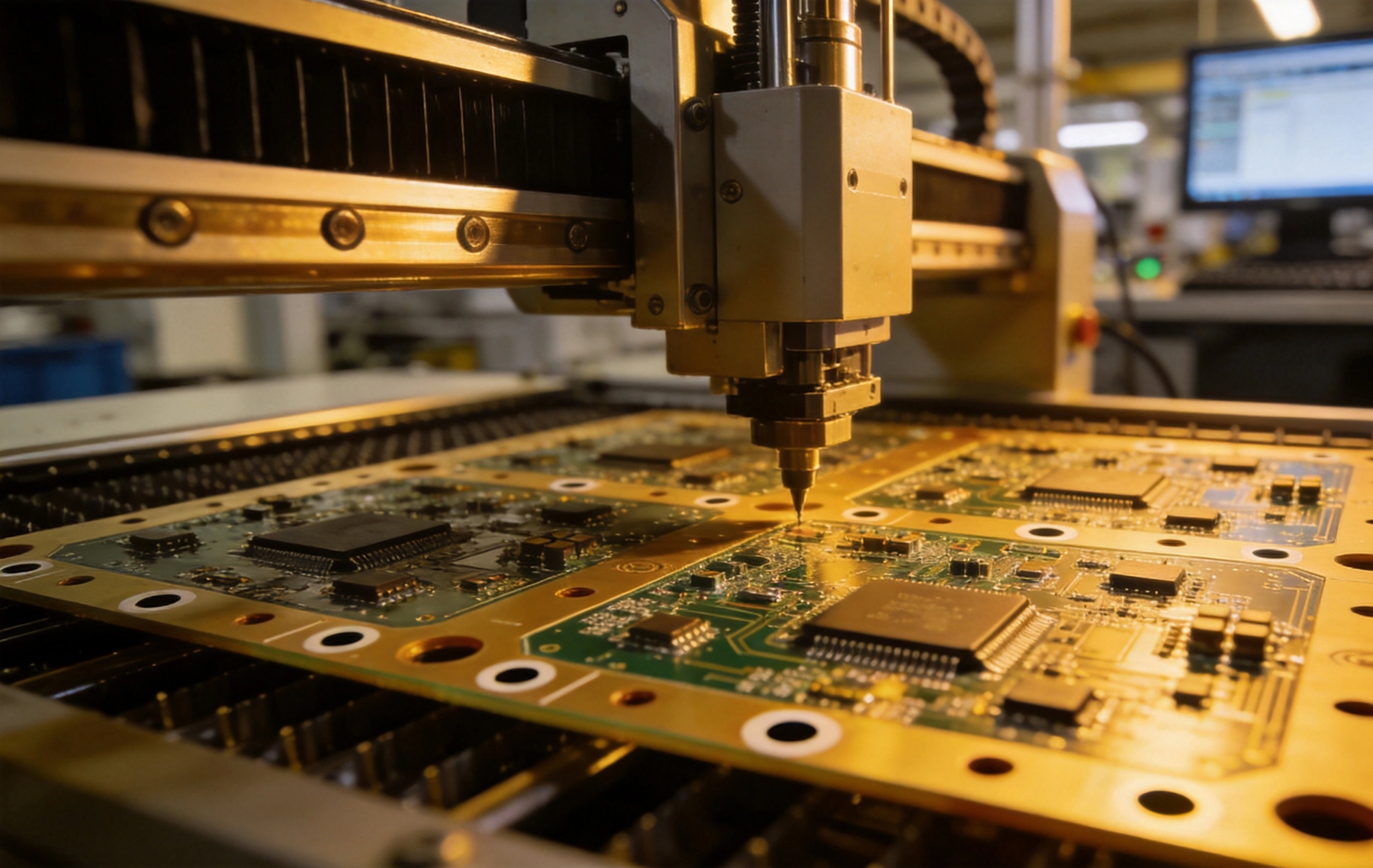
Fiducial marks are precisely positioned reference features on a printed circuit board that serve as alignment points for automated assembly equipment. These distinctive patterns, typically circular or cross-shaped copper pads with contrasting solder mask, enable vision systems in pick-and-place machines, stencil printers, and inspection equipment to accurately locate and orient the PCB during various stages of the assembly process. Think of fiducial marks as the GPS coordinates that guide assembly equipment with micron-level precision.
The fundamental purpose of fiducial marks is to compensate for any mechanical tolerances, thermal expansion, or minor dimensional variations that occur during PCB Fabrication and handling. Even with high-precision manufacturing processes, boards can exhibit slight variations from design specifications. Fiducial marks allow assembly equipment to adapt to these real-world variations dynamically, ensuring that components are placed accurately regardless of minor board-to-board differences that might exist in a production batch.
Fiducial marks typically appear in two forms: global fiducials and local fiducials. Global fiducials are placed near the corners or edges of the PCB and provide overall board positioning and orientation. Local fiducials are positioned near specific components or areas requiring exceptional precision, such as fine-pitch BGAs or QFN packages. This dual-tier approach ensures both overall board accuracy and localized precision for critical components, creating a comprehensive positioning system that addresses different accuracy requirements across the board.
Global fiducial marks serve as the primary reference points for establishing the board's coordinate system and overall orientation. Most assembly equipment requires at least three global fiducials to determine position and rotation unambiguously, though four fiducials placed near the board corners is considered best practice. These global references enable equipment to compensate for board rotation, scaling, and skew, ensuring that the entire component placement pattern aligns correctly with the actual board geometry.
Local fiducial marks provide enhanced positioning accuracy for specific components or regions that demand exceptional precision. These are particularly important for fine-pitch components (pitch less than 0.5mm), BGAs with small ball pitches, or any component where placement accuracy directly impacts electrical performance or reliability. Local fiducials are typically placed adjacent to the component they serve, often as a pair positioned diagonally around the component footprint to provide both position and orientation reference.
Panel-level fiducials are used when multiple PCBs are manufactured and assembled on a single panel. These marks are placed on the panel rails and serve as references for the entire panel during assembly, ensuring consistent positioning across all individual boards on the panel. Panel fiducials are particularly important for maintaining uniformity across high-volume production runs and are essential for processes like panel-level solder paste printing and inspection.
Tooling holes, also known as mounting holes or alignment holes, are precisely positioned non-plated through-holes that serve multiple critical functions throughout the PCB manufacturing and assembly processes. Unlike plated through-holes used for electrical connections, tooling holes remain unplated and are dedicated specifically to mechanical positioning and alignment purposes. These holes provide robust physical references that complement the optical references provided by fiducial marks, creating a comprehensive positioning system that addresses both mechanical and optical alignment needs.
The primary function of tooling holes is to ensure consistent and accurate positioning of the PCB during various manufacturing and assembly operations. During PCB Fabrication, tooling holes align the board for drilling, routing, and other mechanical processes. In the assembly phase, these holes secure the board to fixtures, pallets, or conveyor systems, preventing movement during automated operations. The mechanical nature of tooling holes makes them particularly valuable for applications involving higher forces or where board stability is critical, such as wave soldering or conformal coating processes.
Tooling holes also serve important secondary functions beyond simple positioning. They can act as strain relief points for mechanical connectors, provide mounting points for hardware during final product assembly, and serve as reference points for manual inspection or testing procedures. The versatility and reliability of tooling holes make them an essential feature in virtually all PCB designs, from simple single-sided boards to complex multilayer assemblies.
The design and placement of tooling holes require careful consideration of mechanical tolerances and manufacturing capabilities. Standard tooling holes typically range from 3.0mm to 3.2mm in diameter, which accommodates common locating pins and fixture hardware while providing sufficient clearance for manufacturing tolerances. The hole diameter tolerance should typically be ±0.05mm or tighter, though relaxed tolerances may be acceptable for less critical applications. The positional tolerance of tooling holes is even more critical, with most manufacturers requiring positioning accuracy within ±0.1mm of the nominal location.
Tooling holes should be placed at consistent distances from the board edges, typically 3-5mm from the edge, to ensure reliable engagement with fixture pins while maintaining adequate board material for structural integrity. The distance between tooling holes should be maximized to improve positioning accuracy, with the two primary tooling holes typically placed as far apart as practical, often near opposite corners of the board. This maximized spacing provides the greatest leverage for accurate positioning and rotation control.
Non-plated construction is essential for tooling holes to ensure consistent diameter throughout the hole and to accommodate manufacturing tolerances. Plated holes can vary in diameter due to plating thickness variations, which can compromise the accuracy and reliability of the positioning reference. The absence of plating also prevents any potential issues with solder wicking or electrical shorts that could occur if conductive material entered the positioning hole during assembly processes.
The implementation of properly designed fiducial marks dramatically improves assembly accuracy across multiple dimensions. Modern SMT assembly equipment relies on sophisticated vision systems that capture high-resolution images of the PCB and analyze fiducial mark positions with sub-pixel accuracy. These systems can detect position deviations as small as a few microns and automatically adjust component placement coordinates accordingly. This capability is essential for achieving the placement accuracies required by today's miniaturized components, some of which have feature sizes measured in fractions of a millimeter.
One of the most significant advantages of fiducial marks is their ability to compensate for board scaling and distortion. During the PCB fabrication process, factors such as material shrinkage during lamination, thermal expansion during soldering, and mechanical stresses during handling can cause the actual board dimensions to deviate slightly from the design dimensions. Fiducial marks enable assembly equipment to measure these real-world distortions and apply appropriate scaling corrections to component placement coordinates, ensuring accurate placement despite dimensional variations.
Fiducial marks also provide critical orientation information that prevents board rotation errors. Even a small rotation error of just one degree can cause significant placement inaccuracies for components located far from the origin point. By measuring the positions of multiple fiducial marks, assembly equipment can precisely determine the board's rotation angle and apply appropriate corrections to all placement coordinates. This rotational correction is particularly important for panels containing multiple boards, where small panel rotations can compound into significant placement errors for boards at the panel edges.
Effective fiducial mark design requires attention to several critical parameters that ensure reliable detection and accurate positioning by vision systems. The most common fiducial mark design consists of a solid copper circle, typically 1.0mm to 1.5mm in diameter, surrounded by a clear area devoid of copper traces, pads, or other features. This clear area, known as the keep-out zone, should extend at least 2-3 times the fiducial diameter in all directions to prevent interference from adjacent features that could confuse the vision system.
Contrast is essential for reliable fiducial detection. The fiducial mark should provide high visual contrast against the surrounding board surface. This is typically achieved by leaving the fiducial area exposed copper while covering the surrounding area with solder mask, or vice versa. The choice between exposed copper and solder mask-covered fiducials depends on the specific vision system capabilities and the board's overall solder mask color. Both approaches can work effectively, but consistency across all fiducials on a board is important for reliable detection.
Fiducial marks should be placed on copper layers that are present on both top and bottom sides of the board when both-side assembly is required. For double-sided assemblies, corresponding fiducials should be positioned in the same locations on both sides to enable accurate placement on either side. The registration between top and bottom fiducials should be as precise as possible, typically within 0.05mm, to ensure consistent positioning reference regardless of which side is being assembled.
While fiducial marks provide optical references for vision-based alignment, tooling holes offer robust mechanical positioning that complements and enhances overall assembly accuracy. The physical nature of tooling holes makes them particularly valuable for applications involving higher forces, vibration, or thermal cycling, where purely optical alignment might be compromised. By providing mechanical constraints, tooling holes help maintain board stability throughout the assembly process, from initial loading through final inspection.
In stencil printing operations, tooling holes ensure consistent and accurate positioning of the PCB relative to the stencil, which is critical for achieving uniform solder paste deposition. Even slight misalignment between the board and stencil can cause solder paste to be deposited incorrectly, leading to soldering defects such as bridging, insufficient solder, or misaligned components. Tooling holes that mate precisely with locating pins on the stencil printer fixture eliminate this source of variation, contributing to higher first-pass yields and reduced rework.
During wave soldering or selective soldering processes, tooling holes provide the mechanical stability needed to prevent board movement as the assembly passes through molten solder. The thermal and mechanical stresses of these processes can cause boards to shift if not properly constrained, potentially leading to misaligned components or solder defects. Tooling holes that securely engage with conveyor fixtures or pallets ensure that boards maintain their intended position throughout these demanding processes, preserving assembly accuracy even under challenging conditions.
Optimal tooling hole placement requires balancing multiple factors including positioning accuracy, board utilization, and manufacturing practicality. The two primary tooling holes should be positioned as far apart as practical, typically near opposite corners of the board, to maximize positioning accuracy and rotation control. This maximized spacing provides the greatest leverage for precise positioning, similar to how a wider stance improves balance. However, these holes must also maintain adequate distance from board edges to ensure structural integrity and reliable engagement with fixture hardware.
For rectangular boards, placing tooling holes near the corners along the longer axis generally provides the best combination of accuracy and board utilization. This placement maximizes the distance between holes while leaving adequate space for routing and panelization. For boards with unusual shapes or cutouts, tooling hole placement may require more careful consideration to ensure reliable fixture engagement while avoiding interference with board features or component placements.
Panel-level tooling holes should be positioned on the panel rails rather than on individual boards, ensuring consistent reference points across the entire panel. When designing panels, consider including additional tooling holes along the panel length for larger panels to prevent bowing or flexing during processing. The panel tooling holes should align with standard fixture configurations used by your assembly provider to avoid the need for custom fixtures or workarounds that could increase costs or lead times.
Implementing fiducial marks according to established best practices ensures maximum effectiveness and reliability throughout the assembly process. The most fundamental best practice is to use a minimum of three global fiducials for single-sided boards and four for double-sided assemblies. This number provides redundancy in case one fiducial becomes damaged or unreadable, and it enables the vision system to detect and compensate for board scaling in both X and Y dimensions. Four fiducials placed near the board corners represent the optimal configuration for most applications.
Global fiducials should be positioned as far from each other as practical while maintaining adequate clearance from board edges and features. This maximized spacing improves positioning accuracy by providing the largest possible reference triangle for the vision system to work with. A common approach places fiducials approximately 5-10mm from each board corner, though this distance may need adjustment based on board size and available space. The key principle is maximizing the distance between fiducials within the constraints of board design and edge clearance requirements.
Local fiducials should be placed strategically near fine-pitch components, BGAs, and other packages requiring exceptional placement accuracy. For components with fine pitch (less than 0.5mm), place at least one local fiducial pair within 10-15mm of the component. For BGAs with ball pitches of 0.8mm or smaller, local fiducials become essential for achieving the placement accuracy required for reliable soldering. When multiple fine-pitch components are clustered together, consider placing a single local fiducial pair that can serve the entire cluster rather than individual pairs for each component.
Consistency in fiducial mark design is crucial for reliable detection and accurate positioning. All fiducials on a board should use the same size, shape, and contrast pattern to avoid confusing the vision system. The most effective design is a solid circle, typically 1.0mm to 1.5mm in diameter, with high contrast against the surrounding background. This simple geometric shape provides clear, unambiguous reference points that vision systems can detect reliably across various lighting conditions and board surface finishes.
The keep-out area around each fiducial should be free of any features that could interfere with detection, including traces, pads, vias, or silkscreen markings. This clear zone should extend at least twice the fiducial diameter in all directions, creating a buffer zone that prevents false detections or measurement errors. For a 1.5mm diameter fiducial, the keep-out zone should extend at least 3mm from the fiducial center, ensuring adequate separation from nearby features.
For boards with solder mask, fiducials should be on exposed copper to provide maximum contrast against the surrounding solder mask color. The solder mask should be cleared from the fiducial area completely, with no mask overlap that could reduce contrast or create irregular edges. If your design uses a light-colored solder mask (such as white or yellow), consider using solder mask-covered fiducials with exposed copper background, as this can provide better contrast for some vision systems. Whichever approach you choose, maintain consistency across all fiducials on the board.
Proper tooling hole design ensures reliable positioning and compatibility with standard manufacturing and assembly equipment. The most common tooling hole diameter is 3.175mm (1/8 inch), which accommodates standard locating pins used throughout the industry. This size provides a good balance between accuracy requirements and manufacturing practicality, offering sufficient clearance for tolerance variations while maintaining precise positioning. For applications requiring exceptional accuracy, slightly smaller holes (3.0mm) can reduce positioning play, though this may increase the risk of fit issues if manufacturing tolerances are not tightly controlled.
Tooling holes should be non-plated to maintain consistent diameter and prevent solder wicking or electrical shorts. The non-plated construction eliminates variations in hole diameter that can occur due to plating thickness inconsistencies, ensuring more reliable engagement with locating pins. Additionally, non-plated holes prevent any possibility of solder entering the hole during wave soldering or reflow processes, which could create electrical shorts or interfere with fixture engagement.
The positional tolerance of tooling holes is typically more critical than their diameter tolerance. Most PCB manufacturers can achieve positional accuracy of ±0.1mm or better for tooling holes, though tighter tolerances (±0.05mm) may be specified for applications requiring exceptional precision. When specifying positional tolerances, consider the capabilities of your PCB manufacturer and the actual accuracy requirements of your assembly process. Over-specifying tolerances beyond what's needed can increase costs without providing meaningful benefits.
Tooling holes should be integrated into the board design from the earliest stages rather than added as an afterthought. Consider tooling hole placement when defining board outline dimensions, ensuring that holes maintain adequate clearance from edges and corners while providing maximum spacing for accuracy. Early integration also allows you to coordinate tooling hole locations with other board features, avoiding conflicts with component placements, routing channels, or mechanical constraints.
For boards that will be panelized, coordinate tooling hole placement with panel design to ensure compatibility with standard panel fixtures. Panel-level tooling holes should be positioned on the panel rails rather than on individual boards, and their locations should align with the fixture configurations used by your assembly provider. This coordination prevents the need for custom fixtures or workarounds that could increase costs or lead times, particularly important for high-volume production runs.
Consider including additional tooling holes for boards that will undergo secondary processes such as conformal coating, potting, or mechanical assembly. These additional holes can serve as positioning references for these downstream processes, ensuring consistent accuracy throughout the entire product lifecycle rather than just during the initial PCB assembly. When planning for these additional holes, consider the specific requirements of each process and position holes accordingly to provide optimal positioning for each operation.
One of the most common mistakes in fiducial mark implementation is placing too few fiducials on the board. Some designers attempt to save board space by using only one or two global fiducials, but this approach compromises positioning accuracy and provides no redundancy in case of damage. Always use a minimum of three global fiducials for single-sided boards and four for double-sided assemblies. The additional cost in board space is negligible compared to the benefits in accuracy and reliability.
Another frequent error is placing fiducials too close to board edges or other features. Fiducials placed near edges may be partially cut off during routing or may not provide adequate clearance for fixture hardware. Similarly, fiducials placed too close to traces, pads, or other features can cause detection errors or measurement inaccuracies. Maintain the recommended keep-out distances and edge clearances to ensure reliable fiducial performance throughout the assembly process.
Inconsistent fiducial design across the board represents another common mistake that can cause vision system confusion. Using different sizes, shapes, or contrast patterns for different fiducials on the same board forces the vision system to handle multiple reference types, increasing the likelihood of detection errors or misidentification. Maintain complete consistency in fiducial design across all fiducials on a board to simplify vision system operation and maximize reliability.
Using plated holes for tooling purposes is a fundamental design error that can compromise positioning accuracy. Plated holes vary in diameter due to plating thickness variations, creating inconsistent engagement with locating pins. Additionally, plated holes can wick solder during wave soldering processes, potentially creating electrical shorts or interfering with fixture engagement. Always specify non-plated construction for tooling holes to ensure consistent diameter and reliable performance.
Placing tooling holes too close together significantly reduces positioning accuracy by creating a short baseline for positioning calculations. When tooling holes are closely spaced, small errors in hole position or pin engagement translate into larger angular positioning errors. Maximize the distance between tooling holes as much as practical, typically placing them near opposite corners of the board, to achieve the best possible positioning accuracy.
Neglecting to consider panel-level tooling requirements is another common mistake, particularly for designers who focus only on individual board design. When boards will be assembled on panels, panel-level tooling holes become the primary positioning references, and their placement must coordinate with standard fixture configurations. Failing to consider panel tooling during design can lead to the need for custom fixtures or workarounds that increase costs and complicate the assembly process.
Q: How many fiducial marks do I need on my PCB?
A: For single-sided boards, use a minimum of three global fiducials to establish position and rotation unambiguously. For double-sided boards, use four global fiducials, typically placed near the board corners. Additionally, consider local fiducials near fine-pitch components or BGAs requiring exceptional placement accuracy. This combination provides both overall board positioning and enhanced precision for critical areas.
Q: What's the ideal size for fiducial marks?
A: The most common and effective fiducial size is 1.0mm to 1.5mm in diameter. Smaller fiducials may be difficult for vision systems to detect reliably, especially on boards with surface finishes that reduce contrast. Larger fiducials consume more board space without providing significant accuracy improvements. Choose a size within this range that balances detection reliability with space constraints, and maintain consistency across all fiducials on the board.
Q: Can I use vias as fiducial marks?
A: While vias can theoretically serve as fiducial markers, they're generally not recommended for this purpose. Vias typically have different visual characteristics than dedicated fiducial marks, which can confuse vision systems or reduce detection reliability. Additionally, vias may have plating variations or solder fill that affects their appearance. Use dedicated fiducial marks specifically designed for optical detection rather than repurposing vias for this critical function.
Q: What diameter should tooling holes be?
A: The standard tooling hole diameter is 3.175mm (1/8 inch), which accommodates standard locating pins used throughout the industry. This size provides an excellent balance between accuracy requirements and manufacturing practicality. For applications requiring exceptional precision, 3.0mm holes can be used, though this requires tighter manufacturing tolerances. Avoid using non-standard sizes that may not fit standard fixture hardware.
Q: Do I need tooling holes if I have fiducial marks?
A: Yes, tooling holes and fiducial marks serve complementary purposes and both are typically needed for optimal assembly results. Fiducial marks provide optical references for vision-based positioning, while tooling holes offer mechanical positioning and board stability. Most assembly processes benefit from both types of references, with tooling holes being particularly important for processes involving higher forces, thermal cycling, or vibration where purely optical alignment might be compromised.
Fiducial marks and tooling holes represent fundamental design elements that are essential for achieving accurate, reliable PCB assembly. These features provide the positioning references that enable modern assembly equipment to place components with the precision required by today's miniaturized electronic devices. Understanding their importance, implementing them correctly according to established best practices, and avoiding common design mistakes can significantly improve assembly quality, reduce defects, and lower overall production costs.
The investment in proper fiducial mark and tooling hole design pays dividends throughout the product lifecycle, from initial prototype assembly through high-volume production. By providing reliable positioning references, these features enable higher first-pass yields, reduce rework requirements, and ensure consistent product quality across production runs. In an era of increasing component miniaturization and tighter performance requirements, the importance of these fundamental design elements cannot be overstated.
As you design your next PCB, give careful consideration to fiducial mark and tooling hole implementation from the earliest design stages. Consult with your assembly provider about their specific requirements and recommendations, and incorporate these features as integral design elements rather than afterthoughts. The attention to detail in these fundamental aspects of board design will contribute significantly to the success of your PCBA project and the reliability of your final product.

Smart Factories: The Digital Transformation of PCBA LinesSeptember/17/2026

The Future of Flexible Hybrid Electronics (FHE) in AssemblyAugust/06/2026

Key Terminologies You Need to Know Before Ordering PCB Assembly ServicesSeptember/07/2026

Inventory Management Benefits of Using a Turnkey Assembly PartnerAugust/03/2026

Offshore vs. Domestic PCB Assembly Services: Analyzing the Trade-offsJuly/16/2026