Open Nav


Design for Manufacturability (DFM) is the critical bridge between a flawless schematic and a high-yield, cost-effective production run. In Surface Mount Technology (SMT) assembly, ignoring DFM principles can lead to catastrophic issues such as tombstoning, solder bridging, and component misalignment. By integrating these top 10 DFM tips into your PCB design workflow, you can significantly reduce manufacturing defects and accelerate your time-to-market.
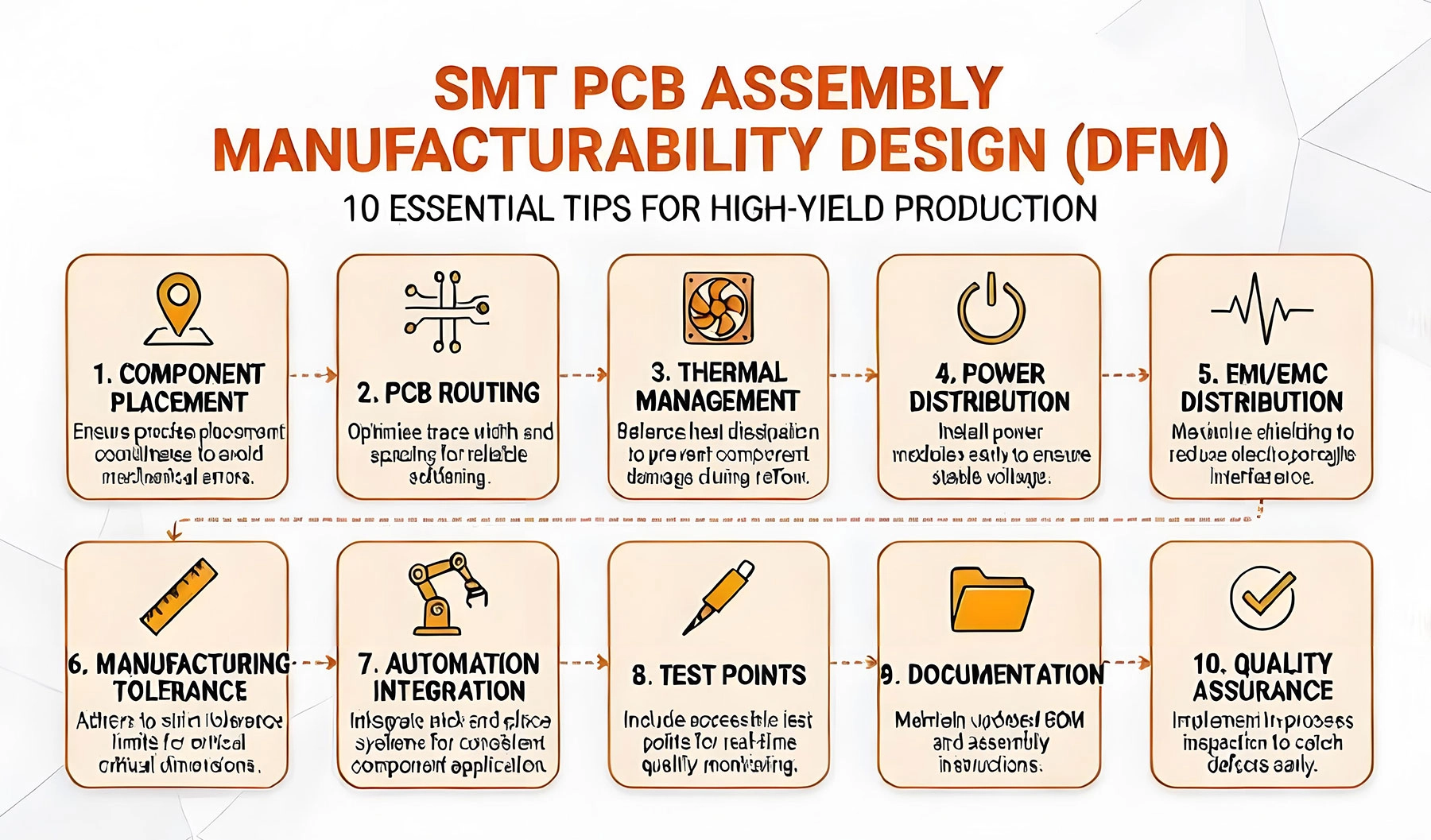
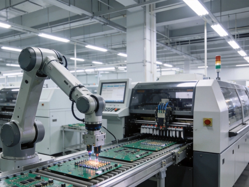
Consistent component orientation is vital for automated pick-and-place machines. Align similar components in the same direction to minimize machine head rotations and reduce cycle times. Furthermore, ensure that components are placed away from board edges and keep a safe distance from each other to prevent mechanical interference during placement and rework.
Pad dimensions dictate solder joint quality. Pads that are too small can lead to insufficient solder and weak joints, while oversized pads can cause tombstoning due to uneven surface tension during reflow. Always adhere to IPC-7351 standards for land patterns and ensure pad sizes match the specific component footprint precisely.
Fiducial marks are the eyes of the SMT assembly line. Include global fiducials on opposite corners of the PCB for board-level alignment, and local fiducials near fine-pitch components like BGAs and QFPs. Ensure these marks are circular, have a high contrast (clear solder mask area), and are not placed on V-cut lines to prevent distortion.
Uneven heat distribution during reflow is a primary cause of solder defects. Avoid placing large copper pours directly connected to small component pads, as the copper will act as a heat sink, leading to cold solder joints. Use thermal relief patterns for standard components, but consider solid connections for high-power components requiring efficient heat transfer.
Your PCB layout must account for the stencil printing process. For fine-pitch components, ensure adequate solder mask dams (at least 0.1mm) between pads to prevent solder bridging. Avoid placing components too close to board edges where the stencil might not seal properly, leading to paste smearing.
Clear silkscreen is essential for both automated optical inspection (AOI) and manual rework. Ensure polarity indicators (diodes, capacitors, IC pin 1) are clearly visible and do not overlap with pads or vias. Keep silkscreen text at a readable size (minimum 0.8mm height) and position it so it won't be hidden by the component body after assembly.
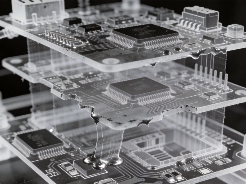
Placing vias directly on SMT pads is a major DFM red flag. During reflow, molten solder can wick down the via hole, resulting in insufficient solder on the pad and potential short circuits on the opposite layer. If a via is absolutely necessary, use via-in-pad technology with resin-filled and copper-plated vias.
Design your PCB with testing in mind. Ensure there is adequate clearance around components so that AOI cameras can capture clear images of all solder joints. Avoid placing tall components directly next to low-profile parts where shadows might obscure the inspection view.
In-circuit testing (ICT) and flying probe testing require accessible test points. Place test points on critical nets, ensuring they are not covered by solder mask or obscured by component bodies. Maintain adequate spacing between test points to prevent shorting during automated testing.
For efficient SMT processing, design your PCB with manufacturability in mind regarding board handling. Include tooling holes (non-plated) for conveyor tracking and fiducial alignment. If using panelization, ensure adequate routing or V-score margins, and add tooling strips (breakaway tabs) if components are placed too close to the board edge.
Applying DFM principles early in the design phase is exponentially cheaper than fixing issues during mass production. By following these top 10 guidelines, hardware engineers can create robust, manufacturable PCB designs that ensure smooth SMT assembly, high reliability, and optimal production yields.
Offshore vs. Domestic PCB Assembly Services: Analyzing the Trade-offsJuly/16/2026
Streamlining Production with Integrated PCB Fabrication and AssemblyJuly/20/2026
Low Volume PCB Assembly: The Bridge Between Prototype and Mass ProductionJuly/07/2026
The True Cost of Poor Quality in PCB Assembly ServicesJuly/13/2026
High-Reliability PCB Assembly Services for Automotive ElectronicsJuly/08/2026