Open Nav



Solder paste inspection, commonly abbreviated as SPI, is one of the most impactful inline quality control technologies in the modern SMT assembly line. Positioned immediately after the paste printing step and before component placement, SPI catches defects at their root cause rather than allowing them to propagate downstream where they become progressively more expensive to fix. A single solder bridge or insufficient paste deposit that goes undetected during printing will, at minimum, require rework once the board reaches functional test. At worst, it reaches the customer and generates a field failure with associated warranty costs and reputational damage.
The economics are straightforward: the cost of fixing a defect multiplies by roughly ten for each stage it travels downstream in the assembly process. A paste print defect caught and corrected before placement costs only the time to reprint. The same defect discovered after reflow requires desoldering, cleaning, reprinting, and re-reflowing. SPI, when properly configured and integrated into the line, provides the earliest possible detection point and the lowest cost-per-defect correction.
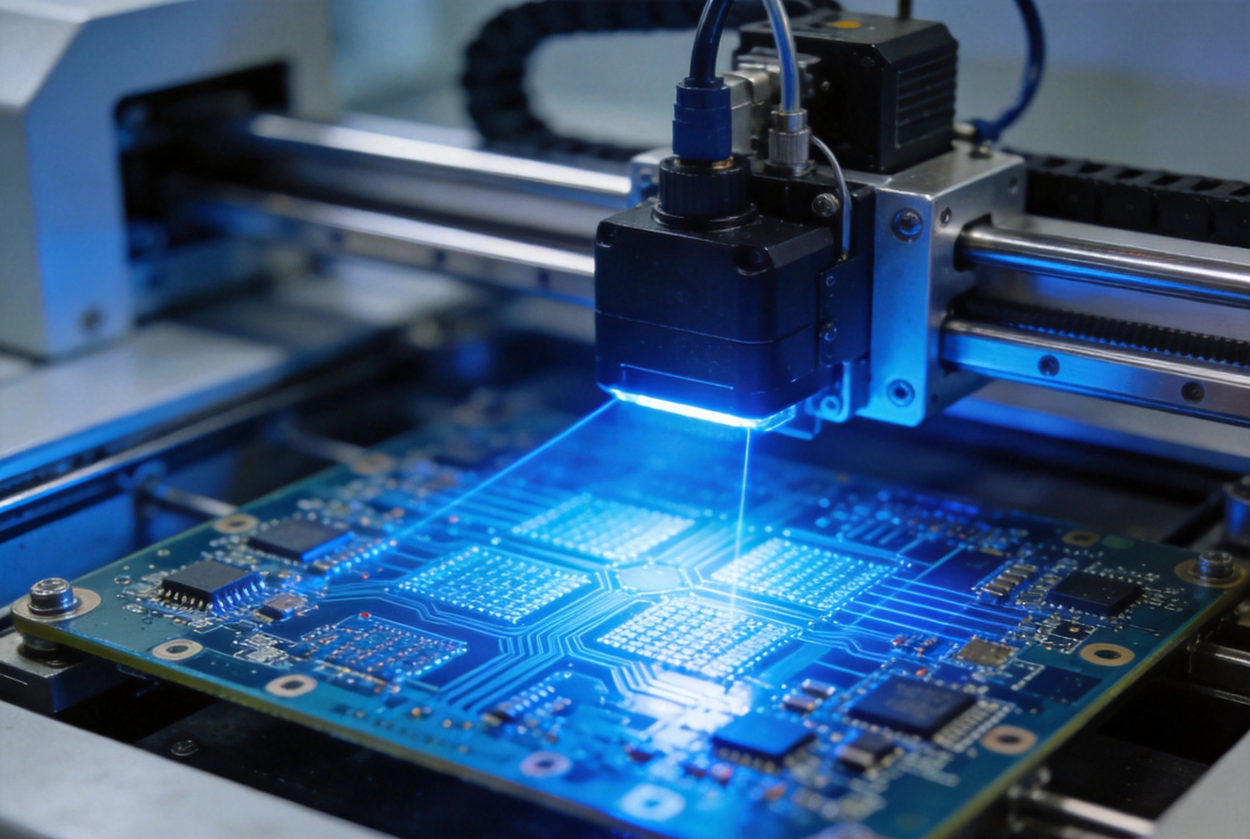
The SMT assembly line follows a well-established sequence: paste printing, component placement, reflow soldering, inspection, and test. SPI sits in the first position of the inspection sequence, directly following the screen printer. Its placement is deliberate. At this stage, the only process that has occurred is the deposition of solder paste onto the board pads. Any defect in paste volume, position, or shape is attributable to one of three sources: the stencil, the printer's squeegee and alignment systems, or the board itself (warped, contaminated, or improperly fixtured).
Because only one process has happened, the failure analysis after an SPI defect detection is simple and fast. If paste volume is consistently low across all components, the likely cause is stencil wear or incorrect squeegee pressure. If it affects only certain components, the cause is more likely pad-specific, such as pad surface oxidation or uneven board support. This immediate diagnostic value is one of SPI's most underappreciated benefits.
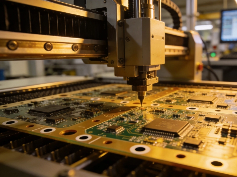
Modern SPI systems capture a three-dimensional map of every solder paste deposit on the board using one of two primary technologies: laser profilometry or structured light projection. Laser-based systems measure height by triangulation, moving a laser stripe across the board surface. Structured light systems project a known pattern of light onto the board and analyze the deformation of that pattern to calculate height and volume. Both approaches can achieve measurement resolutions well below the tolerances required for fine-pitch components.
The key measurements derived from these 3D scans are volume, area, height, and offset. Each measurement is compared against the design intent stored in the CAD data or the paste inspection recipe. The most common defect categories detected by SPI include insufficient paste, excess paste, bridging, smearing, shift, and missing deposits.
Solder paste volume is the single most critical parameter for joint reliability. Too little paste creates a starved joint prone to cracking under thermal cycling or mechanical stress. Too much paste causes bridging between adjacent pads or solder beading on the component side of the board. IPC-A-610 defines acceptable volume ranges as percentages of the nominal paste volume, typically allowing plus or minus 25 to 30 percent for most components, with tighter tolerances for fine-pitch devices.
Beyond volume, the shape of the paste deposit matters. A healthy paste deposit has a slightly domed profile, with the paste well-adhered to both the pad and the aperture walls during printing. A flat or depressed profile may indicate dried-out paste or insufficient squeegee pressure. A slumped profile, where the paste has spread beyond the pad boundary, is a strong predictor of bridging after reflow.
SPI systems measure the X-Y position of each paste deposit relative to the pad. Significant offset indicates printer alignment problems, board fiducial mismatch, or board warpage that shifts the board during printing. Even if paste volume is within tolerance, a deposit that is badly shifted may not adequately wet the pad during reflow, creating an open joint or a head-in-pillow defect with BGA components.
Bridging is one of the most common SMT defects and one of the most reliably caught by SPI. A bridge occurs when solder paste connects two adjacent pads, creating an unintended short circuit after reflow. SPI detects bridging either directly (when the 3D profile shows paste connecting two pad areas) or indirectly (when a paste deposit has a shape inconsistent with its pad footprint). Catching bridging at the print stage eliminates a defect that would otherwise require desoldering and rework.
Poor release from stencil apertures manifests as consistently low paste volumes across all instances of a specific footprint. This is a strong indicator of stencil wear, incorrect surface treatment, or incompatible paste rheology. Without SPI, poor release accumulates undetected until boards reach AOI or ICT, by which time the root cause has generated hundreds of defective boards. With SPI, the trend is visible after the first few boards, enabling rapid corrective action.
While SPI does not directly detect component shift (that is the function of AOI), it detects paste-related conditions that predispose components to shift. Uneven paste distribution under a chip component creates an imbalance in surface tension during reflow, pulling the component toward the side with more paste and causing tombstoning. An SPI system that detects consistently asymmetric paste deposits under chip components provides early warning of a tombstoning risk, even before the first shifted component appears.
Head-in-pillow (HIP) defects occur when a BGA component partially reflows and lifts slightly, creating a void between the solder ball and the paste deposit. The board may pass electrical test initially and fail in the field under thermal stress. SPI reduces HIP risk by ensuring paste volume and deposit shape are optimal, minimizing the conditions that cause the component to lift during reflow. While SPI cannot eliminate all HIP risk, boards with well-controlled paste deposits have significantly lower HIP rates than boards with inconsistent print quality.
Setting up an SPI system requires creating an inspection recipe for each board design. The recipe defines the measurement parameters, tolerance bands, and inspection regions for every component on the board. Modern SPI systems can import CAD data directly, automatically generating component recognition templates and pad definitions from the placement data. This dramatically reduces recipe creation time compared to manual programming.
Tolerance settings must balance detection sensitivity against false alarm rates. Setting tolerances too tight causes the SPI system to flag borderline paste deposits that are within acceptable process variation, generating excessive alerts that slow the line and desensitize operators to real defects. Setting tolerances too loose allows genuine defects to pass undetected. The optimal setting accounts for the actual process capability of the paste printing step, the component sensitivity to paste variation, and the downstream cost of defects escaping to later stages.
Component prioritization is another important recipe decision. Not every component on a board justifies full 3D measurement. Fine-pitch components such as 0201m, 01005, and fine-pitch BGAs require the highest scrutiny. Larger components with wide process windows may be checked with faster 2D profilometry or sampled rather than inspected 100 percent. Effective SPI operation uses a risk-based approach to allocate measurement resources where they deliver the greatest defect detection value.
SPI is most effective when tightly integrated with the screen printer and the process control loop. Closed-loop integration between SPI and the printer allows the system to automatically adjust printer parameters in response to detected deviations. If paste volume trends lower over a production run due to gradual stencil wear, closed-loop adjustment maintains consistent print quality without operator intervention.
The integration can also trigger automatic stencil cleaning cycles. When SPI detects a spike in poor release events across multiple boards, the system can pause the line, initiate a stencil cleaning cycle, and resume production. This prevents the accumulation of hundreds of defective boards while an operator is occupied elsewhere on the line.
Statistical process control (SPC) data generated by SPI systems provides the foundation for continuous improvement in paste printing. Tracking paste volume Cpk (process capability index) over time reveals gradual drift before it becomes a defect problem, enabling preventive maintenance rather than reactive correction. The data also supports root cause analysis when customer returns reveal defects that somehow escaped the SPI station.
SPI has clear boundaries that engineers and quality managers must understand. It inspects paste, not solder joints. A board that passes SPI may still have defects introduced during component placement, reflow, or post-assembly handling. Common SMT defects that SPI does not catch include component placement errors, rotated components, tombstoning (beyond paste-related prediction), insufficient wetting, graping, and pad cratering.
This means SPI is not a replacement for AOI (Automated Optical Inspection) or X-ray inspection downstream. It is a complementary inspection layer that eliminates one major category of defects early in the process, reducing the defect density that subsequent inspection stages must handle. The combined approach of SPI plus AOI plus X-ray (for BGAs and QFNs) provides the most comprehensive quality coverage across the assembly process.
For some procurement teams, the decision to add SPI capability comes down to a simple cost-benefit calculation. Consider a production scenario running 1,000 boards per shift across three shifts daily. Without SPI, even a well-controlled paste printing process with a 99 percent first-pass yield will produce approximately 30 defective boards per shift from print-related causes. Each defective board requires rework at an average cost of USD 15 to 40, plus the risk of latent defects reaching customers.
Adding SPI with closed-loop printer feedback can improve first-pass print yield to 99.5 percent or higher, reducing defect escapes to fewer than 15 boards per shift. The SPI system's cost is amortized across the production volume, and the reduction in rework alone often justifies the investment within months. When the cost of customer returns, warranty claims, and reputation damage is factored in, SPI becomes one of the highest-return quality investments in the SMT assembly line.
Key specifications to evaluate when selecting an SPI system include measurement resolution, repeatability, inspection speed, and software integration capability. Measurement resolution for fine-pitch applications should be 2 microns or better in the Z-axis and 5 microns or better in X-Y, with volume accuracy within 1 percent across the board. Repeatability is as important as resolution: a system that measures inconsistently generates false alarms or misses real defects.
Inspection speed must match the cycle time of the SMT line. For high-volume lines running above 20,000 cph, SPI inspection time becomes a line rate constraint. Systems based on structured light projection typically offer faster measurement than laser profilometers, though both technologies are capable of sub-second inspection times for boards with moderate component counts.
Software features that affect long-term usability include CAD import capability, automatic recipe generation, SPC trending tools, and integration with MES (Manufacturing Execution System) or ERP platforms for traceability. Boards that require traceability data for automotive, medical, or aerospace certifications must record SPI results linked to individual board serial numbers. Not all SPI systems support this level of data granularity.
Solder paste inspection is not a luxury reserved for high-reliability applications. It is a fundamental quality control station that pays for itself through defect reduction in virtually any SMT production environment. By catching print-related defects at the earliest possible stage, SPI eliminates the compounding cost of rework, improves first-pass yield, and provides the process data needed for continuous improvement. When combined with AOI and X-ray inspection downstream, SPI forms part of a comprehensive defect prevention strategy that protects both manufacturing yield and customer satisfaction.
Engineers evaluating their assembly line quality strategy should treat SPI as an essential investment rather than an optional upgrade. The combination of immediate defect detection, process feedback to the screen printer, and statistical data for continuous improvement delivers measurable return on investment in every production scenario, from quick-turn prototyping runs to high-volume mass production.
Modern SPI systems typically inspect a standard board in 5 to 20 seconds depending on component count and measurement settings. High-speed systems designed for high-volume lines can inspect boards with up to 500 components in under 10 seconds. The inspection is performed inline, meaning the board passes through the SPI station and continues to the placement machine without accumulating significant queue time.
No. SPI inspects paste deposits before reflow and cannot detect defects that originate during component placement, reflow soldering, or post-assembly processes. It is most effective at eliminating paste-related defects such as bridging, insufficient paste, and poor release. Defects such as component shift, tombestones, and insufficient wetting require AOI, X-ray inspection, or other downstream inspection methods.
State-of-the-art SPI systems can reliably inspect paste deposits for 01005 (0402m metric) components and fine-pitch devices with pad sizes below 0.2mm. The limiting factor is typically the SPI system's optical resolution and the physical access to paste on extremely dense boards. Most commercially available SPI systems handle 0201 (0402) and larger without difficulty.
Start with IPC-A-610 guidelines as a baseline, then adjust based on the actual process capability of your paste printing line. Run a capability study to measure Cpk for your paste volume process, then set SPI tolerances to match the process capability with appropriate guard band for early detection of drift. Most experienced SPI operators find that tolerances set at ±25 to 30 percent of nominal work well for general components, with tighter settings for fine-pitch and BGA components.
Inline SPI that inspects every board is significantly more effective than offline sampling, which only inspects a statistical subset of production. Sampling can miss systematic drift between inspection intervals, allowing dozens or hundreds of defective boards to accumulate before the next sample is inspected. Inline SPI provides 100 percent coverage and closed-loop feedback to the printer, making it the preferred configuration for production environments where defect escapes carry significant cost.

High-Reliability PCB Assembly Services for Automotive ElectronicsJuly/08/2026
The True Cost of Poor Quality in PCB Assembly ServicesJuly/13/2026
The Hidden Costs of DIY PCB Assembly vs. Professional ServicesAugust/11/2026
Key Terminologies You Need to Know Before Ordering PCB Assembly ServicesSeptember/07/2026
The Importance of Fiducial Marks and Tooling Holes in PCBAAugust/12/2026