Open Nav


The drive toward smaller, lighter, and more powerful electronic devices has shaped the industry for decades, but 2026 marks an inflection point where miniaturization accelerates across nearly every application category. From medical implants delivering therapeutic payloads from spaces smaller than a grain of rice to automotive electronics consolidating dozens of control units into single integrated modules, the boundaries of what is mechanically possible continue expanding. Understanding these trends matters for engineers designing next-generation products, procurement professionals planning component strategies, and business leaders evaluating market opportunities in an increasingly compact electronics landscape.
This article examines the key technological and market forces driving miniaturization in 2026, the assembly techniques making it possible, and the challenges that come with pushing density to unprecedented levels. The convergence of advanced materials, precision manufacturing, and system-level integration is reshaping competitive dynamics across industries ranging from consumer wearables to industrial automation.

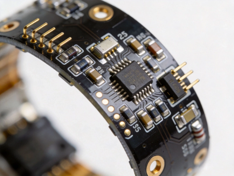
The wearables market continues expanding beyond fitness trackers and smartwatches into continuous health monitoring, augmented reality glasses, and smart clothing with integrated electronics. Each generation of wearable product reduces size and weight while adding capability, creating relentless pressure on assembly engineers to pack more function into smaller volumes. Blood glucose monitoring patches, ECG patches, and drug delivery devices push into medical territory where size directly affects patient comfort and compliance.
Implantable electronics including pacemakers, neurostimulators, and hearing aids have driven miniaturization for decades, but the convergence of sensing, processing, wireless charging, and communication in a single implantable device creates challenges that demand packaging innovations beyond conventional surface mount approaches. Companies developing these products increasingly turn to chip-scale packaging, flexible substrates, and 3D integration to meet volume constraints measured in cubic millimeters.
Modern vehicles contain hundreds of electronic control units managing everything from engine operation to passenger entertainment. Automotive manufacturers face pressure to reduce wiring harness weight and complexity while adding features, creating demand for domain controllers and zonal architectures that consolidate multiple functions into single powerful modules. These consolidated electronics require higher component density than the distributed architectures they replace, driving adoption of advanced packaging techniques previously reserved for consumer electronics.
Electric vehicles amplify this trend through battery management systems, power conversion modules, and charging infrastructure that must handle high power levels while fitting within increasingly compact enclosures. The thermal management challenges in automotive power electronics interact with miniaturization requirements in ways that demand innovative approaches to materials selection, package design, and manufacturing process control.
Industrial sensors and edge computing nodes proliferate across factory floors, warehouses, and infrastructure installations, with many deployments requiring small form factors that blend into existing environments without disrupting operations. Environmental sensors the size of a matchbox must operate for years on single battery charges while performing increasingly sophisticated signal processing and wireless communication tasks. This combination of requirements pushes assembly density while constraining power consumption to milliamps.
Smart infrastructure applications including building automation, structural monitoring, and asset tracking create additional demand for compact electronics that integrate sensors, processing, power management, and radio transceivers in packages optimized for deployment at scale. Cost sensitivity at high volumes drives manufacturing innovations that bring advanced packaging within reach of price points unimaginable just a few years ago.
High Density Interconnect (HDI) PCB technology has evolved from a specialty capability to a baseline expectation across consumer electronics, and its influence continues expanding into industrial and automotive applications. HDI's combination of laser-ablated microvias, fine-line routing, and sequential lamination enables routing densities several times higher than conventional multilayer boards, directly enabling the miniaturization that product designers demand.
Any-layer HDI constructions, where microvias connect any combination of adjacent layers, represent the current state of the art for organic substrate technology. Apple's adoption of any-layer HDI for iPhones demonstrated that these constructions could achieve high-volume manufacturing at consumer price points, and the technology has subsequently proliferated across the industry. Medical devices, industrial sensors, and communication modules now routinely specify any-layer HDI to achieve size targets that conventional board technology cannot meet.
Alternative substrate materials including LTCC (Low Temperature Cofired Ceramic), embedded trace substrates, and flexible hybrid electronics expand the designer's palette for miniaturization. Each material system offers trade-offs between electrical performance, thermal capability, and manufacturing cost that must be evaluated against specific application requirements. The trend in 2026 shows increasing adoption of these specialized materials for applications where standard HDI approaches reach their practical limits.
Component packages continue evolving toward smaller footprints with better electrical and thermal performance. BGA (Ball Grid Array) packages have matured from exotic high-density options to standard components across most application categories. The transition to smaller BGA pitches—0.5mm and below—enables continued area reduction even as traditional package shrink approaches physical limits.
CSP (Chip Scale Packaging) takes miniaturization to its logical extreme, with package dimensions within 20% of the silicon die they contain. These packages present significant assembly challenges due to their thermal expansion mismatch with organic substrates and the difficulty of inspecting concealed solder joints. Yet their size and electrical performance advantages drive adoption in applications from smartphones to medical implants where every cubic millimeter matters.
Fan-out wafer-level packaging (FOWLP) and fan-out panel-level packaging (FOPLP) represent the next frontier in component-level integration. These technologies redistribute connections from the silicon die to a larger package footprint, enabling higher I/O counts and better thermal performance than chip-scale approaches while maintaining compact overall dimensions. Samsung's FOPLP efforts and TSMC's InFO technology demonstrate that these approaches have crossed the threshold from research curiosity to manufacturing reality.
Rigid PCB technology inherently limits miniaturization in applications requiring conformal fit to curved surfaces or repeated mechanical flexing. Flexible printed circuits built on polyimide or polyester substrates address some applications, but true stretchable electronics enable entirely new product categories. Conductive traces deposited using stretchable inks, elastic interconnects spanning gaps between rigid islands, and soft sensor arrays that conform to arbitrary shapes all require assembly techniques that differ fundamentally from conventional surface mount approaches.
Medical patch applications demonstrate the commercial viability of flexible hybrid electronics, combining silicon ICs on flexible substrates with printed sensors, stretchable interconnects, and battery integration in skin-conformal packages. These products require assembly processes that accommodate both rigid component placement and flexible trace printing within single manufacturing workflows.
Resistors and capacitors—the passive components that populate every PCB—continue shrinking even as they maintain or improve performance specifications. The 0201 (0.6mm × 0.3mm) package dominated portable electronics a decade ago, and 01005 (0.4mm × 0.2mm) packages now represent the current standard for high-density applications. In 2026, the industry is beginning the transition toward 008004 (0.25mm × 0.125mm) packages for the most space-constrained designs.
These microscopic components present assembly challenges that would have seemed impossible at larger scales. Placement accuracy must remain within a few micrometers despite package dimensions measured in tenths of millimeters. Paste deposition becomes critical, as the paste volume that seems adequate for 0402 components represents excessive fill for 01005 parts, creating tombstoning and bridging risks. Vision systems must resolve features below 50 micrometers to verify component placement and solder joint formation.
Despite these challenges, the area reduction from 0402 to 01005 packages—approximately 75%—creates compelling incentives for manufacturers capable of handling the process complexity. High-volume consumer products including smartphones and hearables routinely specify 01005 components, and industrial applications increasingly adopt these packages as assembly capabilities improve and cost premiums diminish.
Display technology is undergoing a parallel miniaturization revolution that affects assembly requirements for the modules and driver electronics surrounding the display itself. Micro-LED arrays, with individual LED elements below 100 micrometers, enable displays that are thinner, brighter, and more power-efficient than OLED alternatives, but require mass transfer assembly techniques that differ from conventional SMT entirely.
Micro-OLED displays combining silicon driver ICs with OLED emission layers in a single package create assembly-on-display challenges where conventional PCB approaches must interface with display driver electronics through increasingly miniaturized interconnects. The tight spacing between display pixels and driver contacts demands assembly precision measured in micrometers rather than the tenths-of-millimeters acceptable for conventional PCB assembly.
The semiconductor industry has embraced chiplet architectures as a path beyond the diminishing returns of conventional monolithic silicon scaling. These architectures combine multiple specialized chips in a single package, achieving higher system performance through optimized silicon for each function rather than forcing heterogeneous workloads onto a single general-purpose processor. The packaging complexity shifts from silicon fabrication to assembly operations that must achieve tolerances and yields previously reserved for semiconductor processes.
2.5D interposer packaging using silicon or organic interposers to route connections between chiplets has matured through smartphone applications, and the technology is now proliferating into data center, automotive, and industrial applications. 3D stacking with through-silicon vias (TSV) takes integration further, directly stacking memory on processors or stacking processors on each other to minimize interconnect length and maximize bandwidth while reducing package footprint.
Miniaturization demands placement equipment capable of positioning components with accuracy previously considered unnecessary for electronics assembly. Standard placement tolerances of ±0.1mm suffice for 0402 components but prove inadequate for 01005 packages and fine-pitch BGAs. Advanced placement systems now achieve placement accuracy below ±0.02mm through mechanical design improvements, vision system resolution increases, and real-time closed-loop correction based on board and component fiducial measurements.
Inspection of assemblies at the miniaturization frontier requires resolution beyond what conventional AOI systems can provide. The transition from visible light to UV illumination, higher magnification optics, and specialized lighting techniques enable inspection of features below 20 micrometers. X-ray inspection becomes more critical as ball pitch decreases and BGA packages become the norm rather than the exception, with CT scanning providing the detailed 3D analysis necessary for root cause investigation when defects escape production inspection.
Component density increases thermal concentration, as heat sources occupy smaller volumes and dissipate less efficiently into surrounding structures. Thermal simulation during design becomes essential rather than optional for high-density assemblies, identifying hot spots and thermal coupling paths that could compromise reliability. Materials selection including thermal interface materials, high-Tg substrates, and metal-core constructions must address thermal challenges while fitting within size and cost constraints.
Power density in automotive and industrial power electronics creates thermal challenges that interact with miniaturization pressures. Wide-bandgap semiconductors including silicon carbide and gallium nitride enable power modules that are smaller than silicon alternatives, but their superior efficiency reduces waste heat proportionally, creating thermal design challenges that differ from simply managing more heat output. Advanced packaging including press-fit contacts, direct bonding, and integrated substrates help manage thermal paths in packages designed from the ground up for compact power electronics.
Reliability validation becomes more challenging as miniaturization reduces margin at every level. Smaller solder joints experience higher stress per unit volume during thermal cycling. Thinner dielectric layers in HDI boards tolerate less contamination before developing electrical defects. The failure modes themselves may differ from conventional assemblies, with intermetallic fracture, dielectric delamination, and corrosion appearing at lower defect densities than in larger constructions.
Accelerated life testing protocols developed for conventional assemblies may not adequately stress the failure mechanisms that affect miniaturized products. Thermal cycling profiles optimized for through-hole solder joints prove insufficient for BGA packages. Vibration testing developed for discrete components may not capture the dynamic loading that flexes fine-pitch interconnects. Reliability engineers must develop test protocols specifically targeted at the products they are qualifying, often requiring new test vehicle designs and extended qualification programs.
The shift toward miniaturization reshapes component sourcing strategies as the number of qualified suppliers for leading-edge packages decreases. While 0402 and 0805 components remain commodity items available from dozens of manufacturers, 01005 packages and fine-pitch BGAs require assembly capability that limits production to manufacturers with specialized equipment and process expertise. Procurement teams must increasingly source components and assembly services together rather than treating them as independent purchasing decisions.
Component lead times for advanced packages frequently exceed those for standard components, as manufacturing capacity for leading-edge packages grows more slowly than demand. Qualification cycles for new suppliers are lengthy, given the extensive testing necessary to verify process capability for fine-pitch assembly. These dynamics favor long-term supply relationships and forward contracts over spot purchasing approaches that work adequately for mature component categories.
Miniaturization assembly concentrates in regions with the equipment, skilled workforce, and supply chain infrastructure necessary for high-precision manufacturing. China maintains the largest share of advanced packaging and SMT assembly capacity, with Southeast Asia serving as a secondary hub for companies seeking geographic diversification. India and Vietnam are developing assembly capabilities, but their equipment bases and workforce expertise lag established regions for the most advanced applications.
The geopolitical environment adds uncertainty to supply chain planning for miniaturized electronics. Export controls targeting advanced semiconductor and packaging technology restrict equipment access in ways that could affect manufacturing capability development. Companies increasingly plan for multiple sourcing scenarios, qualifying suppliers in different regions to reduce exposure to regional disruptions that have become more common in recent years.
The miniaturization trend accelerating through 2026 represents both opportunity and challenge for electronics manufacturers. Products become more capable, portable, and integrated as assembly techniques advance, creating market opportunities for companies that master the required technologies. At the same time, the complexity of miniaturized assembly demands investment in equipment, process engineering, and workforce development that strains organizational capabilities not designed for precision manufacturing at the frontier.
The technologies enabling miniaturization span advanced PCB substrates, sophisticated component packages, flexible and stretchable electronics, and chiplet-based semiconductor integration. Each technology domain requires specific expertise, and the most capable manufacturers increasingly offer platform approaches that combine multiple technologies to meet demanding application requirements. Whether building medical implants, automotive controllers, or IoT sensors, product teams must understand how these technologies combine to create competitive products in the miniaturized electronics landscape.
Wearable medical devices, automotive electronics consolidation, and edge computing sensors represent the strongest drivers, but the underlying force is consumer and industrial demand for more capable devices in smaller form factors. The convergence of improved battery technology, more efficient semiconductors, and advanced packaging makes previously impossible size reductions achievable.
HDI technology combines laser-formed microvias, fine-line routing, and any-layer interconnection to achieve routing densities several times higher than conventional multilayer boards. This density enables product designers to include more functionality in smaller packages without sacrificing signal integrity or reliability.
01005 packages (0.4mm × 0.2mm) require placement accuracy below 0.02mm, stencil apertures that manage paste volumes 75% smaller than 0402 packages, and inspection systems capable of resolving features below 50 micrometers. These requirements exceed the capability of standard SMT equipment, requiring investment in advanced placement, printing, and inspection systems.
Chiplet architectures shift integration from PCB-level assembly to package-level assembly, requiring precision placement and connection techniques closer to semiconductor fabrication than traditional SMT. This shift blurs traditional boundaries between semiconductor and electronics manufacturing, with implications for workforce skills, equipment investment, and supply chain organization.
Smaller solder joints experience higher stress concentration during thermal cycling. Thinner dielectrics tolerate less contamination. Failure modes may differ from conventional assemblies, requiring new test protocols and qualification approaches. Reliability engineering must be integrated earlier in product development to address miniaturization-related risks before designs are finalized.
Precision SMT PCB Assembly for Wearable TechnologyJune/16/2026
SMT vs. THT: Understanding the Differences in PCB Assembly TechnologiesMay/19/2026
The Science of Solder Paste Printing Keys to Perfect SMT AssemblyJune/04/2026
Low Volume PCB Assembly for Startups The Ultimate GuideJune/03/2026
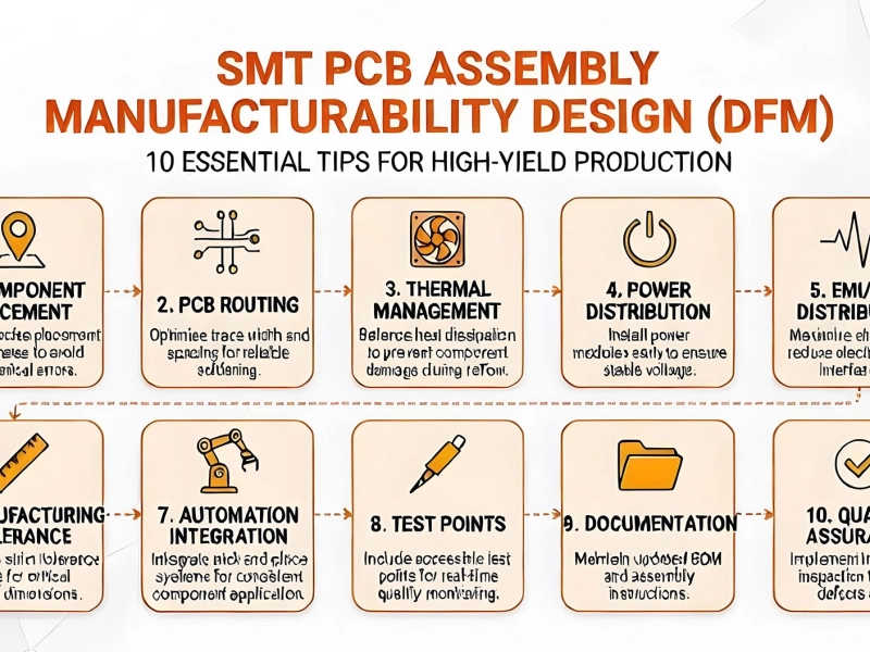
Top 10 DFM (Design for Manufacturability) Tips for SMT PCB AssemblyJune/08/2026