Open Nav


The wearable technology market has exploded in recent years, with smartwatches, fitness trackers, health monitors, and augmented reality glasses becoming everyday companions for millions of users worldwide. Behind every sleek, feature-packed wearable device lies a remarkable feat of engineering: precision SMT PCB assembly that manages to pack sophisticated electronics into spaces smaller than your thumbnail.
As someone who's spent over a decade working with electronics manufacturers in China, I can tell you that assembling PCBs for wearable technology presents a unique set of challenges that push the boundaries of what's possible in surface mount technology. This isn't your grandfather's PCB assembly—we're talking about tolerances measured in microns, components so small they're practically invisible to the naked eye, and quality standards that leave zero room for error.
In this article, we'll dive deep into the world of precision SMT assembly for wearables, exploring the techniques, challenges, and considerations that make this one of the most demanding sectors in modern electronics manufacturing.
Surface mount technology has been the backbone of electronics manufacturing for decades, but wearable applications introduce a whole new level of complexity. When you're designing a PCB for a smartwatch or a medical patch, you face constraints that simply don't exist in traditional applications:
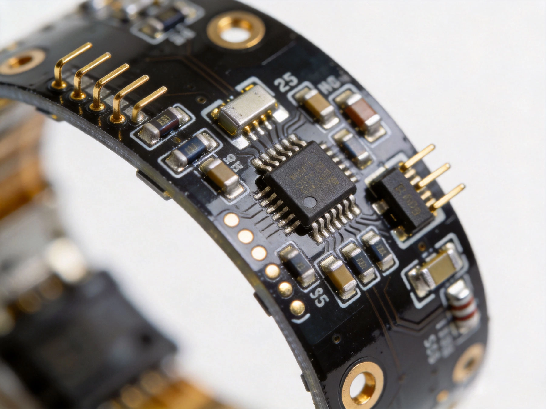
Miniaturization is perhaps the defining characteristic of wearable PCB assembly. While standard consumer electronics might use 0402 (1.0mm × 0.5mm) or 0603 (1.6mm × 0.8mm) passive components, wearables frequently push to 0201 (0.6mm × 0.3mm) or even 01005 (0.4mm × 0.2mm) packages. That's components smaller than a grain of salt.
This miniaturization isn't just about making things smaller—it's about enabling new form factors, improving user comfort, and integrating more functionality into devices people can actually wear. The technical challenges are substantial, but the market rewards are significant.
Wearable devices often require components with pitches of 0.3mm or finer. QFN (Quad Flat No-lead) packages, BGA (Ball Grid Array) components, and fine-pitch SOICs demand placement accuracy measured in microns. Modern SMT lines for wearable assembly use:
The investment in equipment capable of this precision is substantial, which is why not every contract manufacturer can handle demanding wearable assemblies. You need specialized capability, not just general-purpose SMT lines.
Rigid PCBs work fine for many applications, but wearables often need flexibility—literally. Smartwatch bands, hearables, and patches all benefit from flexible circuit technology. Flexible and rigid-flex PCBs present unique assembly challenges:
ul>Manufacturers experienced in wearable assembly have developed specialized fixtures and processes to handle these sensitive substrates. In my experience, the difference between a manufacturer who occasionally does flex and one who specializes in it is night and day in terms of yield and reliability.
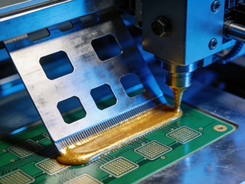
Precision assembly for wearables often requires techniques beyond standard reflow soldering:
Wearables face unique stress conditions that assembly must withstand. Consider what your device will endure: daily charging, body movement, temperature fluctuations, exposure to moisture and sweat. Assembly quality directly determines whether a product lasts 6 months or 3 years.
Key reliability considerations include:
When components are invisible to the naked eye, traditional visual inspection won't cut it. Leading wearable assembly manufacturers employ:
We've found that manufacturers who invest heavily in inspection tend to have better long-term reliability records. The inspection cost is minimal compared to field failures and warranty claims.
Residue on wearable assemblies isn't just a cosmetic concern—it can cause reliability failures. Flux residue, hand oils, and particulate contamination can lead to:
Precision wearable assembly facilities maintain cleanroom environments and use rigorous cleaning processes, including aqueous cleaning, ultrasonic cleaning, and plasma treatment for especially sensitive applications.
Material choice impacts everything from signal integrity to flexibility to biocompatibility:
Wearable assemblies use an increasingly diverse range of component packages:
Not all SMT manufacturers are equipped for precision wearable work. When evaluating potential partners, consider:
The best assembly partnerships start during design, not after. Look for manufacturers who offer DFM reviews that can catch potential issues before production:
Small solder joints under BGAs and QFNs can trap gas during reflow, creating voids that weaken mechanical and electrical connections. Solutions include:
Fine-pitch components are susceptible to misalignment from paste oxidation, uneven heating, or pad design issues. Prevention methods include:
Flexible circuits can be damaged by excessive handling, thermal shock, or mechanical stress during assembly. Best practices include:
Let's address the elephant in the room: precision wearable assembly isn't cheap. The specialized equipment, cleanroom facilities, and experienced personnel required for high-quality work come at a premium. However, the cost equation often makes sense when you consider:
We've seen companies save money upfront by choosing cheaper assembly options, only to spend far more on debugging, reworking, and managing field failures. The total cost of ownership perspective is crucial.
The wearable technology space continues to evolve rapidly, and assembly techniques must keep pace:
Precision SMT PCB assembly for wearable technology represents one of the most demanding applications in modern electronics manufacturing. Success requires specialized equipment, experienced personnel, rigorous quality processes, and careful attention to the unique challenges of miniaturization and flexibility.
When selecting a manufacturing partner for your wearable device, look beyond price to consider true capability, relevant experience, and commitment to quality. The extra investment in precision assembly pays dividends in product reliability, customer satisfaction, and brand reputation.
Wearable technology continues to push the boundaries of what's possible in electronics miniaturization. By understanding the assembly challenges and working with capable partners, you can bring innovative wearable products to market that meet the exacting standards today's consumers expect.
Modern wearable assemblies commonly use 01005 (0.4mm × 0.2mm) passive components, with some applications pushing to 008004 (0.25mm × 0.125mm). Fine-pitch ICs with 0.3mm or finer pitch are also standard.
Reliability is ensured through proper material selection, specialized handling procedures, appropriate flex joint design, thorough inspection including micro-section analysis, and testing that simulates actual use conditions including bend cycling.
At minimum, look for ISO 9001 certification. Medical device wearables should have ISO 13485. Automotive wearables may require IATF 16949. IPC certifications for assembly workmanship are also valuable indicators of quality.
Precision wearable assembly typically costs 20-50% more than standard consumer electronics assembly due to specialized equipment, cleanroom requirements, enhanced inspection, and experienced personnel. However, this premium often represents better value when considering yield and reliability.
Not all can. While many have the basic capability, true precision wearable work requires fine-pitch placement equipment, advanced inspection systems (including X-ray), flex handling expertise, and robust cleanliness controls. Always verify specific capability before committing.
Comprehensive testing typically includes AOI for visual inspection, X-ray for hidden joints, ICT for electrical verification, programming and calibration, functional testing of wireless and sensor systems, and often environmental stress testing for thermal cycling, humidity, and mechanical shock.
Top 10 DFM (Design for Manufacturability) Tips for SMT PCB AssemblyJune/08/2026
Low Volume PCB Assembly for Startups The Ultimate GuideJune/03/2026
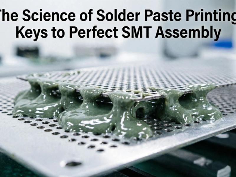
The Science of Solder Paste Printing Keys to Perfect SMT AssemblyJune/04/2026
The Science of Solder Paste Printing: Keys to Perfect SMT AssemblyMay/19/2026
SMT vs. THT: Understanding the Differences in PCB Assembly TechnologiesMay/19/2026