Open Nav



The smart home device market has grown from a niche category of enthusiast gadgets into a mainstream consumer market with hundreds of millions of units shipped annually. Thermostats, door locks, cameras, speakers, plugs, bulbs, sensors, and hubs populate homes across the world, and the companies that compete in this market have discovered that product success depends as much on manufacturing economics as on feature design. A smart home device that is technically superior but costs twice as much as the competitive alternative will not win market share, regardless of its engineering sophistication. Cost-effective assembly for mass markets is not a secondary concern for smart home device companies; it is a primary determinant of commercial viability. Understanding the manufacturing strategies, component selection approaches, and assembly techniques that reduce per-unit cost without sacrificing the reliability that consumers expect from devices that run 24 hours a day, seven days a week, is essential for any company designing or sourcing smart home products.
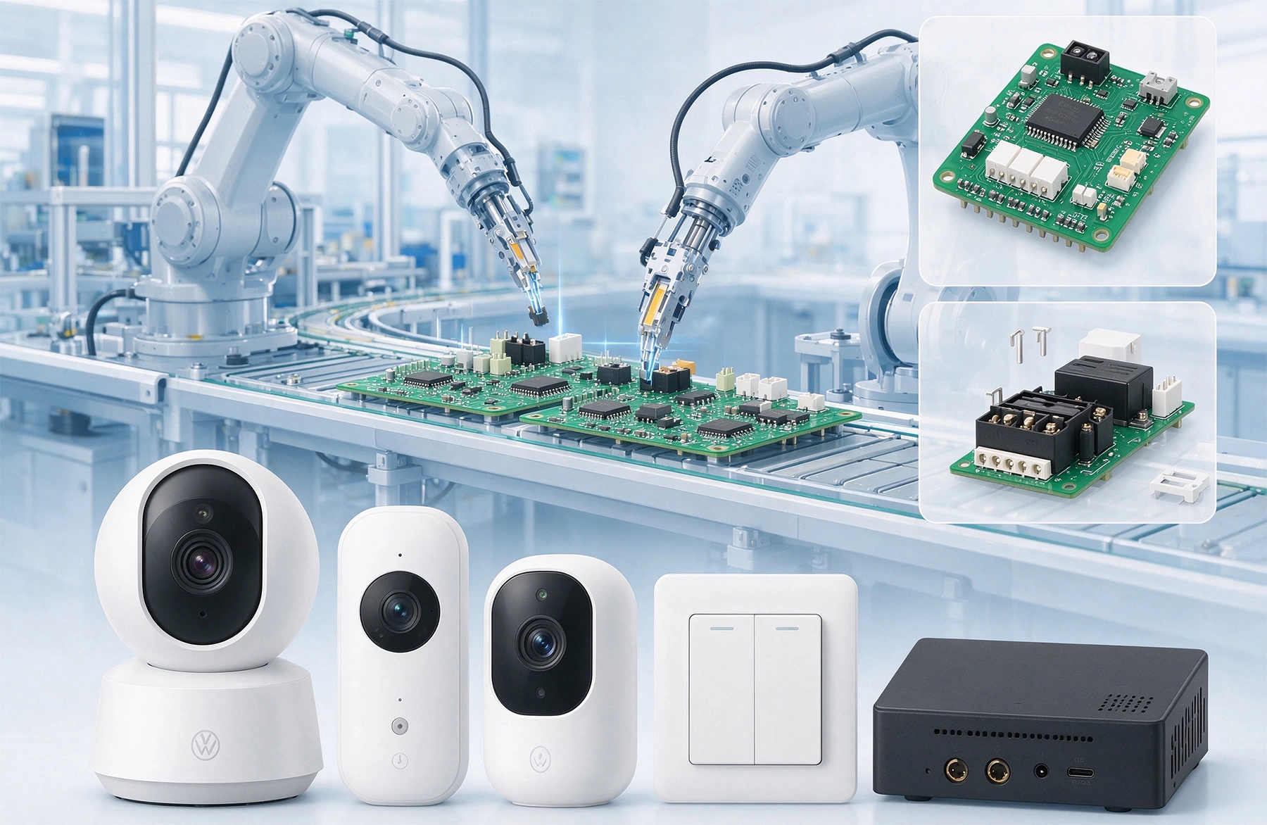
Before reducing cost, it is necessary to understand where the cost originates in a smart home device assembly. The total landed cost of an assembled smart home device consists of several major components, each of which has different levers for cost reduction.
The bare PCB Fabrication cost depends on the board size, the layer count, the material selection, and the feature density. A smart home device typically uses a two-layer or four-layer board, with the layer count determined by the routing density and the shielding requirements of the wireless section. The board area is often the single largest driver of PCB cost because larger boards consume more panel area and reduce the number of boards that can be fabricated per panel. Minimizing the board footprint while maintaining the required functionality is a primary cost reduction strategy, and this drives the adoption of smaller package components and higher routing density. The material selection for smart home devices is typically standard FR-4 or a mid-grade material like IT-180 or S1141, which provide adequate thermal and mechanical performance at a lower cost than high-Tg or specialty materials.
Component cost typically represents 50 to 70 percent of the total assembly cost for a smart home device, making it the largest single cost category and the most important target for cost reduction. The component mix in a smart home device includes a microcontroller or system-on-chip that handles the main processing and wireless functions, a wireless front-end module for Wi-Fi, Bluetooth, Zigbee, Z-Wave, or Thread, passive components including resistors, capacitors, and inductors in various package sizes, and connectors and discrete semiconductors for power management, protection, and interface functions. The microcontroller and the wireless module together can account for 40 to 60 percent of the total component cost, which means that the SoC and module selection has an outsized impact on the total assembly cost.
Assembly labor cost depends on the number of placements, the number of solder joints, the complexity of the assembly process, and the geographic location of the assembly facility. A board with 200 components will cost less to assemble than a board with 400 components, all else being equal, because the placement time and the inspection burden are roughly proportional to the component count. The packaging of the components also affects assembly cost: components on reels are less expensive to place than components in trays or tubes because they can be loaded into the feeder system more quickly. The number of reflow oven passes, which is determined by whether the board has double-sided reflow or requires a separate through-hole wave soldering step, adds process complexity and cost.
Test cost, which includes the cost of in-circuit testing, functional testing, programming, and wireless calibration, is often underestimated in smart home device assembly. A device that requires wireless calibration must be tested in an RF-shielded enclosure with calibrated antenna equipment, which adds significant capital cost and per-unit test time compared to a board that requires only basic continuity testing. The programming cost for devices that require firmware download or security key provisioning can be substantial if the programming time is long or if the programming fixtures are expensive. Optimizing the test flow to minimize the total test time while maintaining adequate coverage is an important cost reduction lever that is frequently overlooked in the initial product design.
The component selection decisions made during the design phase have a larger impact on the total assembly cost than any manufacturing optimization, because those decisions lock in the cost structure for the entire production life of the product. Smart home device companies that achieve cost leadership typically make deliberate, informed component choices that optimize for total cost rather than component unit price alone.
System-on-chip integration reduces the total component count and the board area by combining multiple functional blocks into a single package. The most significant integration trend in smart home devices is the combination of the application processor, the wireless transceiver, the RF front-end, and the power management functions into a single chip or a small multi-chip module. A design that previously required a separate microcontroller, a separate Wi-Fi chip, a separate Bluetooth chip, an RF front-end module, and multiple discrete power management components can be replaced with a single SoC that handles all of these functions in a 10mm by 10mm package. The trade-off is that the highly integrated SoC typically has a higher unit price than the individual chips it replaces, but the lower component count, smaller board area, and reduced assembly complexity often produce a lower total cost at production volumes above a few hundred thousand units per year.
Passive component standardization reduces the variety of parts that must be stocked, simplifies the procurement process, and enables higher volume purchasing of fewer part types. A typical smart home device PCB may contain 80 to 150 unique passive component values, but many of these values differ by only a small amount and could be consolidated to a smaller set of standard values. Standardizing on a smaller set of capacitance values, for example using only E12 series values rather than E24 or E96 series values, enables higher volume purchasing and reduces the number of feeders required on the pick-and-place machine, which reduces the setup time for each production run. The trade-off is that non-standard values may require slightly larger component sizes or slightly different circuit topologies to achieve the desired circuit performance, which may increase the board area or the component cost for individual components.
Package size optimization balances the cost of the component against the impact of the package on the board area and the assembly process. The smallest package sizes, like 0201 resistors and 0402 capacitors, reduce the board area and the material cost of the components themselves, but they increase the assembly cost because they are more difficult to place accurately and are more susceptible to damage during handling. For consumer products with moderate production volumes, 0402 for resistors and 0603 for capacitors are common choices that balance the component cost against the assembly complexity. Larger packages like 0805 or 1206 may be appropriate for components that are handled frequently during the product assembly, like connectors or through-hole components, where the improved durability and easier placement outweigh the slight cost and area penalty.
Wireless module selection whether to use a fully integrated wireless module or to integrate the RF front-end discretely onto the board affects both the component cost and the certification cost. A certified wireless module, which has already passed FCC, CE, and other regulatory testing, eliminates the cost and schedule risk of the certification process for the wireless portion of the device, which can be substantial for a first-time certifier. The module cost is higher than the cost of the discrete components it replaces, but the saved certification cost, faster time to market, and reduced regulatory risk often make the module the more cost-effective choice for production volumes below approximately one million units per year. Above that volume, the cost savings from discrete integration may justify the certification investment, depending on the wireless standard and the target markets.
The design decisions that affect manufacturing cost are made early in the development process, when the cost of changing them is low. Designs that incorporate design for manufacturability principles from the beginning achieve lower assembly costs than designs that address manufacturability as an afterthought.
Panel utilization, the fraction of the fabrication panel that is occupied by production boards, directly affects the PCB Fabrication cost because the fabricator prices based on the panel area consumed, not the individual board area. A board that fits 4 units per panel costs twice as much per unit as a board that fits 8 units per panel, even if the boards are identical. Optimizing the board outline to fit efficiently into the standard panel size used by the assembly house, typically a 18-inch by 24-inch or a 21-inch by 24-inch panel, maximizes the panel utilization and minimizes the per-board fabrication cost. Using a panelized array with depanelization scores or v-grooves enables multiple boards to be fabricated and assembled as a single unit and then separated after assembly, which improves the panel utilization for small boards that would otherwise waste a large fraction of the panel area.
Single-sided assembly, where all components are placed on the top side of the board and only through-hole connectors or large components are on the bottom, eliminates the cost of a second reflow pass and the risk of dislodged components during the second pass. Many smart home devices can be designed with all components on the top side if the board area is sufficient to accommodate the component layout and the connector placement. The board area penalty for single-sided assembly may be 10 to 20 percent compared to a double-sided design, but the saved assembly process cost and the improved first-pass yield often make single-sided assembly the lower total cost option.
Through-hole component elimination, replacing through-hole connectors and components with surface-mount equivalents, reduces the assembly cost by eliminating the wave soldering or hand-soldering step that is required for through-hole parts. Many connectors, including USB connectors, barrel jacks, and pin headers, are available in surface-mount packages that can be placed by the pick-and-place machine and soldered in the reflow oven along with the rest of the components. The surface-mount versions may cost slightly more per unit, but the elimination of the additional assembly step and the wave solder fixture cost typically produces a net cost reduction. For components that must be through-hole for mechanical reasons, like heavy connectors or parts that require high retention force, the through-hole process cost is unavoidable but can be minimized by limiting the count of through-hole parts to only those that genuinely require it.
fiducial marks on both sides of the board, if double-sided assembly is required, enable the placement machine to compensate for panel distortion and improve placement accuracy for fine-pitch components. The cost of adding fiducial marks is minimal, typically a few cents per board for the additional artwork and the panel space, but the improvement in placement accuracy reduces the number of placement errors that require rework. For boards with 0.4mm pitch BGA or QFN packages, accurate fiducial-based placement is essential for achieving acceptable yields without expensive rework operations.
The unit cost of a smart home device decreases as the production volume increases, but the relationship between volume and cost is not linear. Understanding the volume breakpoints where different manufacturing strategies become cost-effective enables companies to choose the right approach for their current volume and to plan for the transition as volume grows.
Prototype and low-volume assembly, for production runs below approximately 500 units per order, is typically performed by quick-turn assembly services that accept small orders with standard pricing. These services use a standardized process with higher per-unit cost than high-volume production, but they do not require the customer to commit to large minimum orders or to invest in production tooling. The cost per unit for a 100-unit prototype build may be 3 to 5 times the cost per unit for a 50,000-unit production run, but the total cost is still manageable because the quantity is small. This approach is appropriate for product development, initial market launch, and demand validation before committing to high-volume production.
Mid-volume assembly, for production runs of 500 to 5,000 units per order, benefits from dedicated production arrangements with an assembly partner who can provide competitive pricing for moderate volumes without requiring the full tooling investment of high-volume production. At this volume level, the assembly house can amortize the setup cost for the specific board across a moderate number of units, reducing the per-board setup cost. The component pricing may still be at standard distribution prices, which are higher than volume contract pricing, but the volume is not yet large enough to justify the procurement commitment required for contract pricing. Mid-volume assembly is a common staging ground for products that are growing from prototype to full-scale production.
High-volume assembly, for production runs above approximately 5,000 units per order, unlocks volume pricing from component distributors and assembly houses, as well as the possibility of moving production to lower-cost geographies like Southeast Asia where the labor cost per placement is lower. At high volumes, the assembly house can invest in dedicated tooling, including custom stencils, production fixtures, and test fixtures, that reduce the per-board process cost. The component distributor can offer contract pricing that is 10 to 30 percent below standard distribution pricing in exchange for the volume commitment and the forecasting accuracy that high-volume production provides. The total unit cost reduction from moving from mid-volume to high-volume production can be 20 to 40 percent, depending on the component mix and the assembly location.
The component supply chain for smart home devices affects both the unit cost and the supply risk. A component that is sourced from a single supplier at a low price creates supply risk that could disrupt production; a component that is dual-sourced from approved suppliers at a slightly higher price provides supply security. Balancing cost and supply risk through thoughtful supply chain design reduces the total cost of ownership beyond the component unit price.
Long-term component agreements with key suppliers, particularly for the high-cost components like the SoC and the wireless module, lock in pricing for a defined volume over a defined period in exchange for volume commitments and forecast accuracy. These agreements provide pricing that is 5 to 15 percent below spot pricing, which can represent significant savings on components that cost several dollars each. The trade-off is that the company must commit to the volume forecast and accept the consequences if the actual demand deviates significantly from the forecast. Over-committing to components that cannot be used creates inventory obsolescence cost; under-committing forfeits the pricing benefit and may leave the company at the back of the allocation queue during shortages.
Component second-source qualification, the process of qualifying an alternate supplier for a critical component, provides supply chain resilience at a small cost premium. The qualification process includes verifying that the alternate component is functionally equivalent, electrically compatible, and physically interchangeable, and updating the BOM to reflect both approved sources. The per-component cost for second-sourcing is typically 2 to 5 percent of the component price, paid as an NRE to the assembly house for the BOM update and the process verification. The benefit is that if the primary source experiences allocation, shortage, or discontinuation, the company can switch to the alternate source without a lengthy qualification process or a production interruption.
Component lifecycle management, monitoring the lifecycle status of each component on the BOM and planning for end-of-life transitions before they become urgent, prevents the production disruptions and last-time-buy cost premiums that occur when a component reaches end-of-life without warning. Many semiconductor manufacturers provide product change notifications and end-of-life notices 12 to 18 months before the last shipment date, but these notices are only useful if the company has a system for receiving and acting on them. A component lifecycle monitoring process that tracks the status of each BOM component and triggers a qualification action when a component enters the notice period enables a planned, controlled transition to an alternate part rather than a crisis-driven scramble to qualify a replacement under time pressure.
The test strategy for a smart home device balances the cost of test against the quality risk of shipping defective units. An under-tested device risks field failures, warranty returns, and reputation damage; an over-tested device carries unnecessary cost that makes it less competitive. Optimizing the test strategy requires understanding what defects are most likely, what their cost is if they escape to the field, and what test coverage is necessary and sufficient to achieve the target defect rate.
In-circuit testing verifies that each component on the board is present, correctly placed, and correctly soldered by measuring the electrical characteristics of the component in-circuit. An ICT fixture with spring-loaded test probes contacts test points on the board and measures the resistance, capacitance, and voltage at each test point, detecting open solder joints, shorted joints, missing components, and wrong component values. The cost of the ICT fixture, which can range from $5,000 to $50,000 depending on the board complexity and the test point count, is amortized across the production volume. For high-volume smart home devices, ICT is cost-effective because the per-board test cost is low when amortized over large volumes and the defect detection coverage is high. For low-volume devices, the fixture cost per board may be prohibitive, and a flying probe tester, which uses movable probes instead of a dedicated fixture, may be more cost-effective despite its higher per-board test time.
Functional testing verifies that the assembled device performs its intended functions, including the wireless connectivity, the sensor operation, the actuator control, and the cloud communication. Functional test is more expensive than ICT because it requires the device to be fully powered, programmed, and exercised through its operating modes, but it detects defects that ICT cannot, including firmware loading errors, calibration problems, and wireless performance issues. A functional test station for a smart home device typically includes a power supply, a programming interface, a wireless test system or a wireless test chamber, and test software that automates the test sequence and records the results. The test station cost and the per-unit test time determine the per-board functional test cost, which should be optimized to minimize the total cost of test including the cost of escaping defects.
Burn-in testing, operating the device under power at an elevated temperature for an extended period, accelerates the failure of components with latent defects that would fail in the field after a short operating time. The burn-in cost is the cost of the power, the thermal chamber, and the labor to load and unload the boards during the burn-in period, which typically ranges from 4 to 48 hours depending on the reliability requirements and the component quality level. For consumer smart home devices, burn-in testing is not always cost-effective because the cost of the burn-in may exceed the warranty cost that would be incurred if a small percentage of units fail early in the field. For commercial or industrial smart home devices, where the cost of a field failure is higher and the reliability expectations are greater, burn-in testing may be justified despite its cost.
The assembly partner is not just a vendor; it is a strategic resource whose capabilities, reliability, and pricing directly affect the competitiveness of the smart home device. Managing the relationship effectively, including setting clear expectations, sharing information transparently, and incentivizing continuous improvement, produces better outcomes than a purely transactional supplier relationship.
Clear technical communication, providing the assembly partner with complete and accurate design data including the BOM, the gerber files, the assembly drawings, and the test specifications, prevents the misunderstandings and errors that arise from incomplete information. The BOM should include the full part number, the manufacturer, the quantity per board, and the reference designator for every component. The gerber files should be current and consistent with the BOM, with no discrepancies between the PCB layout and the assembly drawing. The test specifications should define the test coverage, the test limits, and the disposition criteria for failing units. Providing this data in a standardized format through a controlled release process ensures that the assembly partner is always working from current information.
Yield visibility, tracking the first-pass yield and the final test yield for each production run and sharing the data with the assembly partner, enables collaborative problem-solving when yields fall below target. A first-pass yield below 95 percent indicates a process problem that is costing money for both the company and the assembly partner, because each reworked board consumes additional labor and material. Sharing the yield data transparently and discussing the root cause of any yield loss creates a shared incentive to improve the process, the component quality, or the design for manufacturability. An assembly partner who provides detailed yield reporting and proactively escalates yield concerns is demonstrating the operational transparency that supports a productive long-term relationship.
Cost reduction roadmapping, working with the assembly partner to identify and implement cost reduction opportunities over time, keeps the product cost competitive as the market evolves. The initial production cost is rarely the optimal cost; as the production volume grows, as the component market prices change, and as the assembly process matures, opportunities emerge to reduce the unit cost through higher volume pricing, process optimization, and design simplification. A quarterly cost review with the assembly partner, identifying the largest cost contributors and the most promising reduction opportunities, ensures that cost reduction is an ongoing activity rather than a one-time event. The assembly partner's engineering team can often suggest design or process changes that reduce cost without affecting quality, because they see the manufacturing details more clearly than the design team does.
Cost reduction efforts sometimes backfire, producing short-term savings that create larger long-term costs. Recognizing these common mistakes helps avoid them.
Specifying the lowest-cost component without verifying the second-source availability or the lifecycle status creates supply risk that can disrupt production or require expensive redesign if the component is discontinued or allocated. The component selection process should always include a second-source review and a lifecycle status check, regardless of whether the primary source is the lowest-cost option. A component that costs 5 percent less but has no second source and is scheduled for end-of-life in 18 months is more expensive over the product lifetime than a component that costs 5 percent more but has multiple approved sources and a stable lifecycle.
Aggressively negotiating the assembly price below the assembly partner's cost structure creates a relationship where the partner has no incentive to invest in quality or continuous improvement. If the assembly price does not cover the partner's cost plus a reasonable margin, the partner will either refuse the business, reduce the service level to cut costs, or cross-subsidize from other programs in ways that may not be visible. A fair price that enables the partner to earn a reasonable margin produces better outcomes than a price that wins the business but leaves the partner searching for ways to reduce their cost at the customer's expense.
Skipping the qualification testing to reduce cost and time-to-market creates the risk of shipping devices with undiscovered defects that require expensive field remediation. The qualification testing should include the ICT, the functional test, and the wireless calibration that are required to verify the device meets its specifications. Shortcuts like reducing the burn-in time, skipping the wireless calibration, or reducing the ICT coverage may reduce the immediate test cost but increase the total cost of ownership when the defect escape rate rises.
Cost-effective assembly for smart home devices at mass-market volumes requires a holistic approach that integrates component selection, design for manufacturability, supply chain management, test strategy, and partner relationship management into a coherent cost reduction program. No single tactic produces the dramatic cost reductions that mass-market competition requires; instead, the cumulative effect of dozens of small improvements across each of these areas produces a total cost that is competitive in a market where margins are thin and volume is everything.
The companies that succeed in the smart home market are those that treat manufacturing cost as a first-class engineering discipline, not an afterthought to be delegated to the procurement team after the design is complete. The design decisions made in the first weeks of a project, including the SoC selection, the component package sizes, the board layer count, and the test strategy, determine the cost structure for the entire production life of the product. Making those decisions with full awareness of their cost implications, rather than optimizing purely for performance or schedule, produces products that are both technically excellent and commercially competitive.
Contact us to discuss your smart home device assembly requirements and explore how our PCBA manufacturing capabilities can support cost-effective mass-market production.

How the Global Chip Shortage is Impacting PCB Assembly ServicesJuly/23/2026

Top 10 DFM (Design for Manufacturability) Tips for SMT PCB AssemblyJune/08/2026

Quality Assurance Across the Entire Turnkey PCB Assembly ProcessOctober/15/2026

Advancements in Solder Paste Technology Transforming Electronics ManufacturingSeptember/03/2026

Industrial Control Boards: Heavy Copper and Robust Assembly TechniquesSeptember/29/2026