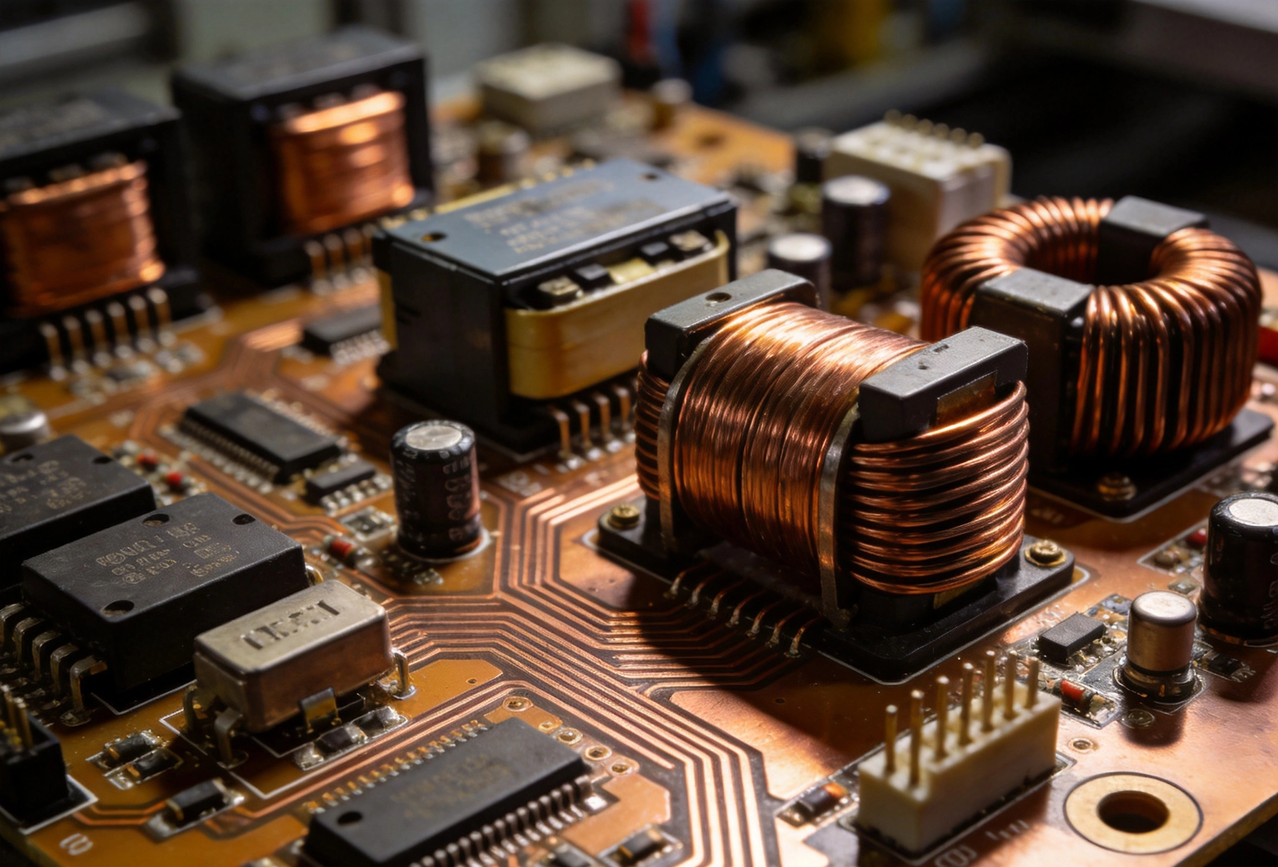
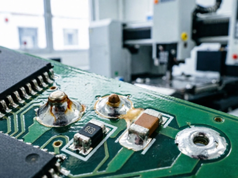
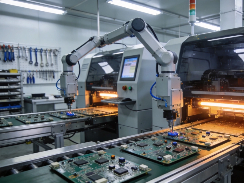
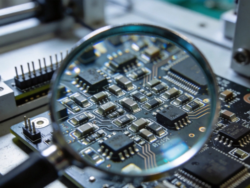
Industrial control boards operate at the intersection of high power and harsh environments, driving motors, switching heavy loads, regulating power conversion, and monitoring processes in factories, power plants, transportation systems, and infrastructure. These boards must carry high currents, withstand extreme temperatures, endure constant vibration, and resist exposure to dust, moisture, and corrosive chemicals—often for 15-20 years without failure. Standard PCB designs and assembly processes used for consumer electronics simply cannot meet these demands. Heavy copper construction and robust assembly techniques are the foundation of reliable industrial control boards, and understanding these specialized approaches is critical for any engineer designing electronics for industrial applications.

Why Industrial Control Boards Need Heavy Copper
Standard PCBs typically use 1-2 oz copper (35-70μm thickness), which is adequate for signal traces carrying milliamps of current but wholly insufficient for power traces that must carry tens or even hundreds of amps. Heavy copper PCBs use copper weights of 3 oz or more per square foot, with the most demanding industrial applications requiring 6 oz, 10 oz, or even 20 oz copper (210μm to 700μm thickness).
The Critical Role of Copper Thickness
- Current Carrying Capacity: Copper thickness directly determines how much current a trace can safely carry without overheating. A 1 oz copper trace 10mm wide can carry approximately 3A with 10°C temperature rise, while a 10 oz copper trace of the same width can carry over 30A—roughly proportional to the copper weight.
- Thermal Management: Heavy copper traces act as integrated heat spreaders, conducting heat away from power components and distributing it across the board surface. This reduces component junction temperatures and improves reliability without requiring additional heat sinks or cooling hardware.
- Mechanical Strength: Thick copper traces and planes provide significantly greater mechanical strength, resisting deformation from thermal cycling, vibration, and mechanical shock that would crack or delaminate thin copper traces.
- Reduced Voltage Drop: Lower resistance in heavy copper traces minimizes voltage drop across power distribution paths, ensuring stable voltage delivery to components and reducing power waste through resistive heating.
- Improved EMC Performance: Heavy copper ground planes provide superior electromagnetic shielding and return path management, reducing radiated emissions and improving immunity to external electromagnetic interference common in industrial environments.
Heavy Copper PCB Design Considerations
Designing with heavy copper requires special attention to several factors that differ significantly from standard PCB design practice:
Trace Width and Spacing
- Heavy copper traces require wider minimum spacing between traces and pads due to increased copper thickness. Etch factors (the ratio of lateral etch to vertical etch) are more pronounced with thick copper, requiring compensation in trace width design.
- For multi-oz copper designs, the etch factor can reduce trace width by 1-2 times the copper thickness. Designers must add this compensation to ensure the finished trace meets minimum width requirements.
- Inner layer registration becomes more critical with heavy copper, as misalignment between layers can cause short circuits or reduced clearance between power and signal traces.
Layer Stackup Strategy
- Many industrial control boards use a mixed copper weight approach, with heavy copper (6-20 oz) on power and ground layers and standard copper (1-2 oz) on signal layers. This optimizes both power handling and signal integrity while managing manufacturing cost.
- Proper stackup design places heavy copper layers symmetrically to minimize board warpage during lamination and thermal cycling.
- Embedded copper technology can place heavy copper power planes in internal layers, freeing outer layers for component placement and signal routing.
Via and Interconnect Design
- Standard vias cannot reliably carry the high currents present in heavy copper power paths. Power vias must be designed with increased copper plating thickness, larger via diameters, or multiple vias in parallel (via arrays) to handle the current.
- Via-in-pad construction is common for power components, using filled and capped vias beneath component thermal pads to transfer both current and heat to internal power planes.
- Conductive via filling with copper paste or electroplated copper provides both electrical continuity and thermal transfer through the via, with significantly lower resistance than standard unfilled vias.
Robust Assembly Techniques for Industrial Control Boards
Beyond the PCB substrate design, the assembly process must be equally robust to ensure reliable operation in industrial environments:
1. Solder Paste and Reflow Process Optimization
- High-Temperature Solder Alloys: Industrial applications often require high-temperature solder alloys (SAC305, SnAg3.5, or specialty alloys) that maintain joint integrity at elevated operating temperatures. Lead-free SAC305 provides a melting point of approximately 217°C, compared to 183°C for traditional SnPb eutectic solder.
- Optimized Reflow Profiles: Heavy copper boards have significantly higher thermal mass than standard PCBs, requiring extended soak times and carefully controlled reflow profiles to ensure uniform heating and reliable solder joint formation across the entire board.
- Nitrogen Atmosphere Reflow: Nitrogen reflow atmospheres improve solder wetting, reduce oxidation, and produce shinier, more reliable solder joints—particularly important for heavy copper boards with large thermal pads where achieving complete wetting is more challenging.
- Double-Sided Reflow Considerations: Components on the bottom side must withstand a second reflow cycle without falling off. Heavy components may require selective soldering or adhesive bonding in addition to reflow soldering.
2. Through-Hole and Mixed Technology Assembly
- Selective Soldering: Many industrial boards combine SMT components with through-hole components (high-power connectors, large capacitors, transformers, terminal blocks) that cannot be reflow soldered. Selective soldering machines provide precise, automated soldering of through-hole joints without affecting adjacent SMT components.
- Pin-in-Paste (Intrusive Reflow): For moderate-power through-hole components, pin-in-paste technology deposits solder paste in through-hole barrels and reflows both SMT and through-hole joints simultaneously, improving throughput and joint reliability.
- Wave Soldering: For boards with many through-hole components, wave soldering remains a cost-effective option but requires careful process control to avoid bridging on densely spaced connections and thermal shock to sensitive SMT components.
3. High-Reliability Solder Joint Requirements
- IPC-A-610 Class 3 Standards: Industrial control boards typically require Class 3 acceptance criteria, the most stringent IPC workmanship standard, which permits minimal defects and requires nearly perfect solder joint formation.
- Solder Volume and Fillet Requirements: Heavy copper pads and large component leads require significantly more solder volume to achieve proper fillet formation and joint strength. Solder paste stencil design must be carefully optimized with increased aperture sizes and appropriate stencil thickness (often 0.15-0.20mm for industrial boards).
- Thermal Cycling Reliability: Industrial environments subject boards to thousands of thermal cycles over their service life. Solder joints must be designed with adequate stand-off height and fillet size to accommodate the differential expansion between components and the PCB without fatigue cracking.
4. Conformal Coating and Environmental Protection
- Conformal Coating: Industrial control boards almost always require conformal coating to protect against moisture, dust, chemical contamination, and fungal growth. Common coatings include acrylic (AR), silicone (SR), polyurethane (UR), and epoxy (ER), each offering different levels of protection, reworkability, and thermal performance.
- Selective Coating Application: Automated selective coating machines apply coating only where needed, leaving connectors, test points, and adjustable components uncoated while ensuring complete coverage of solder joints and circuit traces.
- Potting and Encapsulation: For extreme environments (outdoor exposure, submersible applications, high-vibration installations), potting compounds provide complete encapsulation of the board and components, offering maximum environmental and mechanical protection.
- Coating Inspection and Validation: UV-fluorescent coating materials enable automated inspection under UV light to verify complete coverage and detect thin spots, pinholes, or uncovered areas that could lead to corrosion failures.
5. Mechanical Reinforcement Techniques
- Underfill for BGA Components: BGA packages on industrial boards require underfill adhesive to reinforce solder joints against thermal cycling and vibration stresses. No-flow and capillary flow underfills are selected based on the specific reliability requirements and rework considerations.
- Component Adhesive Bonding: Heavy components (large inductors, transformers, electrolytic capacitors) that could be dislodged by vibration are secured with structural adhesives or mechanical fasteners in addition to solder joints.
- Strain Relief for Cables and Connectors: Cable connections to industrial boards require strain relief mechanisms (cable clamps, tie-down points, right-angle connectors) to prevent mechanical stress from being transferred to solder joints.
- Board-Level Mechanical Support: Additional mounting points, stiffener bars, and mechanical brackets prevent board flexing that could crack solder joints on heavy components during vibration or shock events.
6. Testing and Quality Assurance
- In-Circuit Testing (ICT): ICT verifies individual component values and solder joint integrity for all components, catching opens, shorts, and incorrect values before boards leave the manufacturing floor.
- Functional Testing Under Load: Industrial boards must be tested under realistic electrical loads to verify performance at rated current and voltage levels. Power cycling tests verify that the board can handle repeated turn-on and turn-off transients without damage.
- Hipot (High Potential) Testing: Verification of insulation integrity between high-voltage circuits and low-voltage/safety circuits is mandatory for industrial boards operating at mains voltages or higher.
- Environmental Stress Screening (ESS): Temperature cycling and vibration screening of 100% of production units catches latent defects (weak solder joints, marginal components) before shipment, significantly reducing early-life field failures.
- 3D X-Ray Inspection: For high-reliability industrial boards, 3D X-ray inspection verifies hidden solder joints under BGA and QFN packages, confirms via filling quality, and detects internal defects in heavy copper layers.
Common Industrial Control Board Applications
- Motor Drives and Inverters: Variable frequency drives (VFDs) and servo motor controllers that switch hundreds of amps at high switching frequencies, requiring heavy copper for power stages and robust thermal management for IGBT and MOSFET modules.
- Power Supplies and Converters: Industrial power supplies, DC-DC converters, and battery management systems for factory automation, telecommunications, and energy storage systems.
- PLC and I/O Modules: Programmable logic controller I/O modules that interface between low-voltage control logic and high-voltage industrial field devices, requiring robust isolation and high-current output stages.
- Protection Relay Systems: Electrical protection relays for power distribution systems that must operate reliably for decades in substation environments with extreme electrical and environmental stresses.
- Welding and Heating Controllers: High-power controllers for resistance welding, induction heating, and similar applications that handle extreme currents and temperatures.
Manufacturing Challenges and Solutions
Heavy copper and robust assembly present specific manufacturing challenges that experienced industrial PCB manufacturers have developed solutions for:
- Etching Uniformity: Heavy copper etching requires optimized etchant chemistry, agitation, and process control to achieve uniform etching across the panel. Differential etching (multiple copper weights on the same layer) requires additional process steps and tighter controls.
- Lamination Quality: Laminating boards with heavy copper layers requires higher press pressures and optimized prepreg selection to ensure complete resin fill between heavy copper features and prevent voids or delamination.
- Solder Paste Printing: The varied pad sizes on industrial boards (tiny signal pads alongside massive power pads) require specialized stencil designs, often using step stencils with different thicknesses in different areas to optimize paste deposition for both fine-pitch and large power components.
- Inspection Complexity: The wide range of component sizes and solder joint types on industrial boards makes automated inspection more challenging, requiring configurable AOI systems and multiple inspection passes with different parameter settings.
Conclusion
Industrial control boards demand far more from their PCB substrates and assembly processes than consumer electronics. Heavy copper construction provides the current carrying capacity, thermal management, and mechanical strength needed for reliable operation in harsh industrial environments, while robust assembly techniques including specialized soldering, conformal coating, mechanical reinforcement, and comprehensive testing ensure that every board meets the stringent reliability requirements of industrial applications. By understanding and properly implementing these heavy copper and robust assembly techniques, engineers can design industrial control electronics that deliver years of dependable service in the most demanding operating conditions.
Contact us to discuss your requirements.