Open Nav


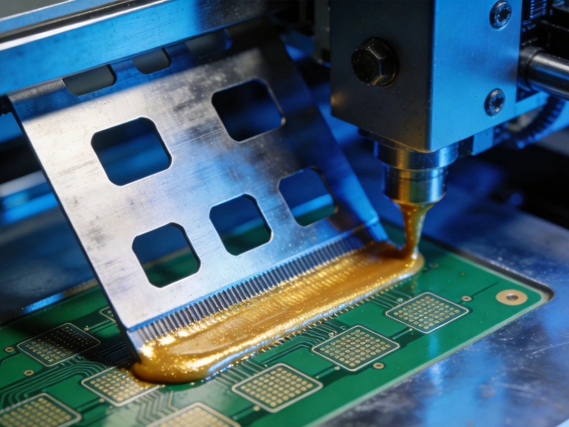
Surface Mount Technology (SMT) has revolutionized electronics manufacturing, enabling the production of compact, high-density electronic devices. However, the precision required in SMT processes introduces various potential defects that can compromise product quality and reliability. Understanding these common SMT defects and implementing preventive design measures is crucial for engineers and manufacturers seeking to achieve high assembly yields and robust electronic products.
SMT defects generally fall into several categories based on their origin: design-related issues, material-related problems, process variations, and environmental factors. While some defects stem from manufacturing process parameters, many can be prevented through proper design for manufacturability (DFM) practices. The most common SMT defects include cold solder joints, tombstoning, solder bridging, solder balling, component misalignment, and non-wetting issues. Each defect type has specific characteristics, root causes, and prevention strategies that designers should understand.
Modern SMT assembly achieves impressive density - for instance, 0201 components can be mounted within 1cm² for 25 components. This high density, however, demands exceptional precision and control throughout the manufacturing process. Even minor deviations in design or process parameters can lead to significant defect rates. By implementing comprehensive prevention strategies at the design stage, manufacturers can dramatically reduce defect rates and improve overall assembly quality, with some studies showing potential yield improvements of 20-30% when proper DFM practices are followed.
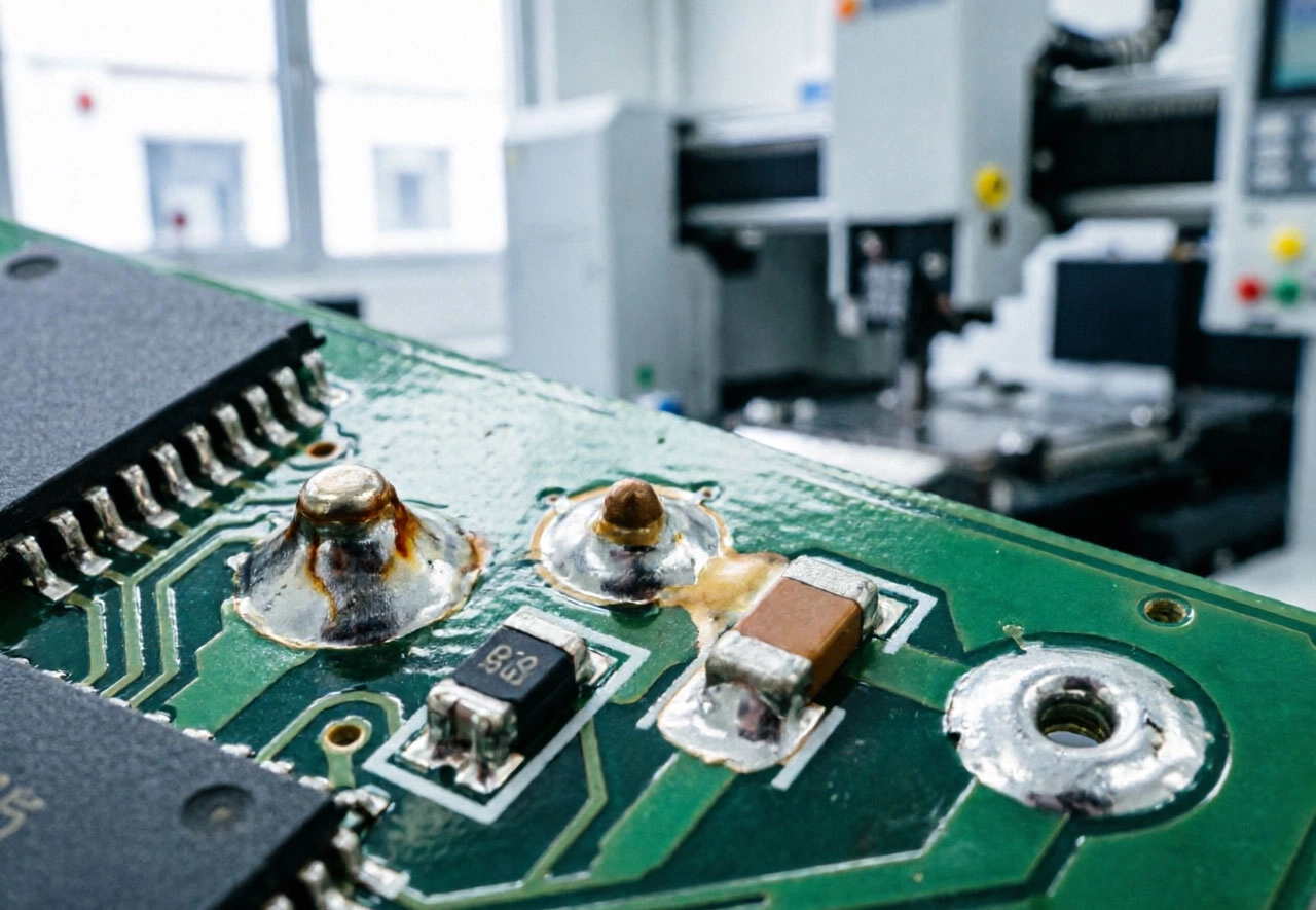
Cold solder joints represent one of the most insidious SMT defects, often remaining undetected until field failures occur. These defects manifest as dull, grainy, grayish-white solder joints that lack proper wetting and mechanical strength. The characteristic appearance resembles "tofu dregs," providing visual evidence of incomplete solder reflow. Cold joints typically result from insufficient reflow temperature profiles, inadequate thermal energy transfer, or issues with solder paste activity.
Primary causes include improper reflow temperature profiles with insufficient peak temperature or time above liquidus, excessive heating rates that prevent proper solder wetting, and oxidation of component leads or PCB pads. Other contributing factors include inadequate solder paste activity, thermal imbalances across the assembly, and variations in component thermal mass. In some cases, cold joints occur when different areas of the same board experience significantly different thermal profiles during reflow.
Designers can prevent cold solder joints by implementing thermal-aware design practices. This includes ensuring consistent thermal mass across the board through proper copper balancing, avoiding large thermal sinks near small components, and incorporating thermal relief pads where appropriate. PCB stack-up design should optimize thermal conductivity while maintaining signal integrity. Component placement should consider thermal profiles, grouping similar thermal mass components together when possible. Design rules should specify appropriate pad sizes and shapes that promote proper solder joint formation and ensure adequate thermal exposure during reflow.
Tombstoning, also known as "drawbridging" or "Manhattan effect," occurs when a surface mount component stands upright during reflow, with one end properly soldered and the other detached from its pad. This defect primarily affects small chip components like resistors and capacitors, especially 0402, 0201, and smaller sizes. The phenomenon results from uneven wetting forces between the two terminations, creating a moment that lifts one end of the component like a seesaw. Tombstoning can cause immediate functional failures and create reliability issues in surviving assemblies.
The tombstoning mechanism stems from surface tension forces during solder reflow. When solder melts, it wets both component terminations and their corresponding pads. If wetting occurs asymmetrically—due to differences in pad size, thermal mass, or solder volume—the stronger wetting force pulls harder on one side, causing the component to pivot. This effect becomes more pronounced with smaller components where the moment arm is shorter, making them more susceptible to even minor force imbalances. The defect typically occurs during the liquidus phase of the reflow profile when surface tension forces are highest.
Effective tombstone prevention requires careful attention to pad design, thermal management, and component selection. Designers should implement symmetric pad designs with size differences not exceeding 10% between the two terminations of each component. For components near large copper areas or ground planes, incorporate thermal isolation features such as thermal relief patterns or "teardrop" pad designs to reduce thermal imbalances. Pad spacing should follow component manufacturer recommendations precisely, with proper solder mask definitions to control solder volume. When working with very small components, consider using pad designs that incorporate solder paste volume control features to ensure consistent solder distribution across both terminations.
While design focuses on prevention, process optimization also plays a crucial role in tombstone reduction. Stencil design should use appropriate area ratios for small components—typically 0.8:1 for 0201/0402 devices—to prevent excessive solder volume on one side. Reflow temperature profiles should include adequate preheat and soak stages to minimize thermal gradients across the board. Heating rates should be controlled to prevent rapid temperature differentials that can exacerbate wetting imbalances. For challenging designs, consider using nitrogen reflow atmospheres to reduce oxidation and improve wetting consistency.
Solder bridging occurs when solder creates unintended connections between adjacent conductors, typically between component leads or pads. This defect can cause short circuits, electrical malfunctions, and in severe cases, component damage. Bridging is particularly problematic in fine-pitch components, BGA (Ball Grid Array) devices, and high-density board areas where conductor spacing is minimal. The defect manifests as visible solder connections that should not exist according to the circuit design.
Solder bridging commonly results from excessive solder paste volume, inadequate solder paste release from stencil apertures, or insufficient spacing between conductive features. Process factors contributing to bridging include solder paste printing issues such as overprinting, smear, or misalignment. Component placement tolerances can also play a role when components shift during reflow. In some cases, solder mask defects or inadequate coverage allow solder to flow into unintended areas. Reflow profile issues, particularly excessive wetting time or improper ramp rates, can also contribute to bridging problems.
Designers can prevent solder bridging through careful layout optimization and appropriate design rules. Maintain adequate spacing between component pads based on component pitch and assembly capabilities. For fine-pitch components, consider implementing solder mask-defined (SMD) pads rather than non-solder mask-defined (NSMD) designs, as SMD pads provide better control over solder spread. Incorporate solder mask webs between adjacent pads when space permits. Pad shapes should follow component manufacturer recommendations, avoiding designs that encourage solder migration between terminations. For BGA devices, consider appropriate via-in-pad designs with proper solder mask control to prevent ball migration.
For extremely dense designs or challenging component geometries, implement advanced design techniques. These include specialized pad designs with reduced surface areas in bridge-prone locations, incorporation of solder mask dams between adjacent pads, and use of thermal relief patterns that control solder flow. Some designers implement "finger-style" pad designs for fine-pitch ICs, which help control solder wetting and reduce bridging potential. Consider using design rules that automatically flag potential bridging issues based on component pitch, pad spacing, and assembly process capabilities.
Solder balling refers to the formation of small, spherical solder particles that appear near solder joints or across the PCB surface. While individual solder balls may seem inconsequential, they can cause significant problems including electrical shorts, reliability issues under thermal cycling, and aesthetic defects in consumer products. Solder balls typically range from microscopic sizes to several hundred microns in diameter and can occur anywhere on the board surface, though they're most common near component leads and in areas with excess solder paste.
Solder balling originates from several mechanisms during the reflow process. Common causes include solder paste oxidation, excessive moisture content in solder paste, incomplete activation of flux, and rapid heating that causes solder paste splattering. Stencil design issues such as insufficient aperture wall smoothness or improper aspect ratios can contribute to paste release problems that lead to balling. Component placement issues, including excessive placement pressure or misaligned components, can also cause solder paste displacement and subsequent ball formation. In some cases, solder mask defects or contamination allow solder to adhere to non-solderable areas.
Design prevention focuses on creating conditions that minimize solder ball formation potential. Ensure adequate solder mask coverage and definition around all pads. Implement proper pad-to-mask spacing to provide solder containment during reflow. Consider solder mask materials with appropriate surface energy characteristics to discourage solder adhesion outside designated areas. For designs prone to solder balling, incorporate solder mask features such as dam structures between adjacent pads. Pad designs should follow component manufacturer recommendations for size and shape, avoiding designs that encourage solder overflow or splatter.
While design provides the foundation, proper material selection and process optimization are essential for solder ball prevention. Specify solder paste with appropriate particle size distribution for the component pitch and pad dimensions. Ensure proper solder paste storage and handling procedures to prevent oxidation and moisture absorption. Stencil design should incorporate appropriate aperture designs with smooth sidewalls and proper area ratios to ensure clean paste release. Reflow profiles should include appropriate preheat stages to activate flux gradually and minimize thermal shock. Consider implementing nitrogen reflow atmospheres for challenging designs to reduce oxidation and improve solder wetting behavior.
Component misalignment occurs when components are not properly centered on their pads or shift during reflow, potentially causing electrical issues, mechanical stress, or reliability problems. This defect ranges from minor positional offsets that may not affect functionality to severe misalignments that prevent proper soldering. Component displacement during reflow—sometimes called "tombstoning lite"—can occur when components move due to surface tension forces or thermal expansion differences.
Component misalignment sources include pick-and-place machine accuracy limitations, solder paste volume variations, thermal expansion coefficient mismatches, and surface tension forces during reflow. High-density designs with small components are particularly susceptible to misalignment issues due to tighter tolerances. PCB warpage or dimensional instability during reflow can also contribute to component displacement. In some cases, component package design or lead geometry can affect positioning accuracy during reflow.
Implement design rules that provide appropriate positional tolerances for all components based on package type and manufacturing capabilities. Use pad designs that incorporate self-alignment features where appropriate—these can include slight pad size variations that encourage components to center during reflow. Ensure adequate solder paste volume to provide sufficient surface tension for proper positioning but not so much that it causes floating or excessive movement. Consider component placement density and spacing to minimize thermal gradients that can cause differential expansion and component shifting. For challenging components, implement fiducial markers or optical alignment targets to improve placement accuracy.
Non-wetting occurs when solder fails to properly bond to metal surfaces, resulting in incomplete or unreliable solder joints. De-wetting describes a related condition where solder initially wets a surface but then retracts, leaving poor solder coverage. Both defects compromise electrical and mechanical connections, potentially leading to field failures. These issues can affect component leads, PCB pads, or through-hole barrel surfaces, creating reliability problems that may not be immediately apparent during electrical testing.
Non-wetting and de-wetting stem from surface contamination, oxidation, or incompatible surface finishes. Common causes include oxidation of component leads or PCB pads due to improper storage or handling, contamination from oils, fluxes, or other processing materials, and surface finish compatibility issues. Inadequate flux activity or improper flux selection can also contribute to wetting problems. Thermal profile issues during reflow can prevent proper flux activation and oxide removal. In some cases, surface finish aging or environmental exposure over time can degrade wetting characteristics.
Specify appropriate surface finishes for all solderable surfaces based on the application requirements and assembly process. Common finishes include ENIG (Electroless Nickel Immersion Gold), HASL (Hot Air Solder Leveling), OSP (Organic Solderability Preservatives), and immersion tin or silver. Each finish has different wetting characteristics, shelf life, and compatibility with different solder alloys. Design rules should specify acceptable surface finishes and storage requirements. Consider implementing gold flash on edge connectors or frequently accessed areas to maintain solderability. For long-term storage or environmental exposure requirements, specify finishes with robust solderability preservation characteristics.
Proper storage and handling specifications play a crucial role in preventing wetting issues. Define appropriate storage conditions for components and PCBs, including temperature, humidity, and packaging requirements. Specify shelf life limits for surface finishes and solder paste. Implement handling procedures that minimize contamination risk, including requirements for gloves, anti-static measures, and environmental controls. For moisture-sensitive components, define appropriate bake-out procedures before assembly. Consider implementing just-in-time delivery strategies for sensitive components to minimize storage time and degradation of solderability.
Effective prevention of SMT defects requires a comprehensive Design for Manufacturability (DFM) approach that addresses multiple aspects of the design process. Implementing robust DFM strategies involves collaboration between design, manufacturing, and quality engineering teams to identify potential issues early and implement preventive measures. Successful DFM implementation can reduce defect rates by 30-50% while improving overall product reliability and reducing time-to-market.
Establish comprehensive design rules that address all aspects of SMT assembly quality. These rules should cover component placement and spacing, pad design, trace routing, solder mask requirements, and thermal management. Design rules should be based on manufacturing capabilities, component specifications, and industry standards. Regular review and update of design rules ensures they remain current with evolving technologies and manufacturing processes. Implement automated DRC (Design Rule Checking) tools to identify potential issues early in the design cycle.
Utilize simulation tools to predict potential assembly issues before production. Thermal simulation can identify temperature gradients that might cause tombstoning or other defects. Solder paste printing simulation can help optimize stencil design and predict bridging risks. Mechanical stress simulation can identify potential reliability issues related to component placement and board geometry. Implement 3D board simulation capabilities to visualize component placement and identify potential interference or assembly challenges.
Conduct regular design reviews with manufacturing engineering teams to identify potential issues and implement preventive measures. These reviews should occur at multiple stages throughout the design process, from concept through final layout validation. Involve representatives from assembly, testing, and quality assurance to ensure comprehensive consideration of all manufacturing aspects. Document all design decisions and rationale to support future design iterations and continuous improvement efforts.
SMT defects remain a significant challenge in electronics manufacturing, but understanding their causes and implementing effective prevention strategies can dramatically improve assembly quality and product reliability. By focusing on design for manufacturability and addressing potential issues before production begins, manufacturers can achieve substantial yield improvements and reduce overall production costs. The investment in proper design practices and preventive measures pays dividends in reduced rework, improved first-pass yields, and enhanced product reliability.
Successful SMT defect prevention requires a holistic approach that integrates design excellence, material science, process optimization, and quality control. Each aspect of the assembly process—from initial PCB design through final inspection—contributes to overall quality. By implementing the strategies outlined in this guide, designers and manufacturers can create robust, reliable electronic products that meet the demanding requirements of modern applications across consumer, industrial, automotive, and aerospace markets.
As component sizes continue to shrink and assembly densities increase, the importance of proper design for manufacturability becomes even more critical. Staying current with evolving technologies, materials, and best practices ensures continued success in SMT assembly quality. Partner with experienced manufacturers who understand both design and process requirements, and invest in the tools and expertise needed to implement comprehensive defect prevention strategies. The result will be higher quality products, reduced costs, and improved market competitiveness in an increasingly demanding electronics marketplace.
Cold solder joints rank among the most common and problematic SMT defects due to their potential to cause field failures that aren't immediately apparent during electrical testing. These defects result from insufficient reflow temperature or improper thermal profiles and can be prevented through proper design for manufacturability practices, including thermal balancing, appropriate pad design, and component placement considerations. Other common defects include solder bridging in fine-pitch applications and tombstoning in miniature components.
Preventing tombstoning requires careful attention to pad design, thermal management, and process optimization. Implement symmetric pad designs with size differences not exceeding 10% between terminations. Incorporate thermal relief features near large copper areas to minimize thermal imbalances. Use appropriate stencil design with proper area ratios for small components. Optimize reflow profiles to minimize thermal gradients. For challenging designs, consider nitrogen reflow atmospheres and advanced pad designs that incorporate solder volume control features.
Solder bridging typically results from excessive solder paste volume, inadequate spacing between conductors, or process issues such as overprinting or misalignment. Prevention strategies include maintaining adequate spacing between pads based on component pitch, using solder mask-defined pad designs for fine-pitch components, incorporating solder mask webs between adjacent pads, and following component manufacturer pad recommendations. Process optimization including proper stencil design, accurate solder paste printing, and appropriate reflow profiles also helps prevent bridging.
Solder balls form from mechanisms including solder paste oxidation, excessive moisture content, incomplete flux activation, and rapid heating causing paste splattering. Prevention involves proper solder paste selection and handling, appropriate stencil design with smooth aperture walls, adequate solder mask coverage, optimized reflow profiles with proper preheat stages, and consideration of nitrogen reflow atmospheres for challenging designs. Proper pad design and solder mask specification also help contain solder and prevent ball formation.
Surface finish selection significantly impacts wetting behavior, solder joint quality, and long-term reliability. Different finishes—ENIG, HASL, OSP, immersion tin, and immersion silver—offer varying solderability characteristics, shelf life, and compatibility with different solder alloys. Proper finish selection based on application requirements and assembly process requirements helps prevent non-wetting issues and improves overall solder joint quality. Consider storage requirements, environmental exposure, and long-term solderability preservation when selecting surface finishes.

Reflow Soldering Profiles Explained: Avoiding Thermal DefectsJuly/01/2026
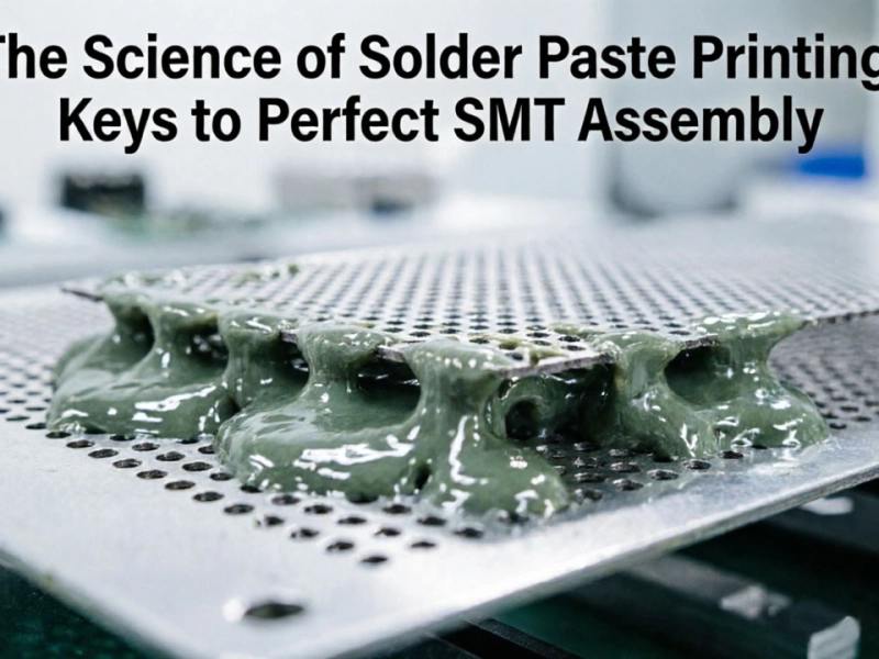
The Science of Solder Paste Printing Keys to Perfect SMT AssemblyJune/04/2026
SMT vs. THT: Understanding the Differences in PCB Assembly TechnologiesMay/19/2026
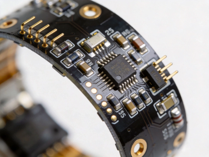
Precision SMT PCB Assembly for Wearable TechnologyJune/16/2026
The Science of Solder Paste Printing: Keys to Perfect SMT AssemblyMay/19/2026