Open Nav



PCB assembly costs do not start and end with component pricing. The way your boards are arranged on a manufacturing panel has a direct, measurable impact on what you pay per finished unit. Panelization, the practice of arranging multiple PCB units onto a single panel for assembly processing, is one of the most underappreciated levers in production cost optimization. Get it right and you shave pennies off every unit. Get it wrong and you pay a premium that compounds across every board you order.
Most engineering teams understand panelization at a surface level: put more boards on a panel, run the assembly line once, and split the setup cost across more units. That much is obvious. What is less obvious is how the specific choices made during panelization — the panel size, the routing or scoring method, the amount of rail space reserved for tooling, the spacing between units — interact with your contract manufacturer's capabilities and your product's specific requirements. Those interactions create both savings opportunities and hidden cost traps that are easy to fall into without a clear strategy.
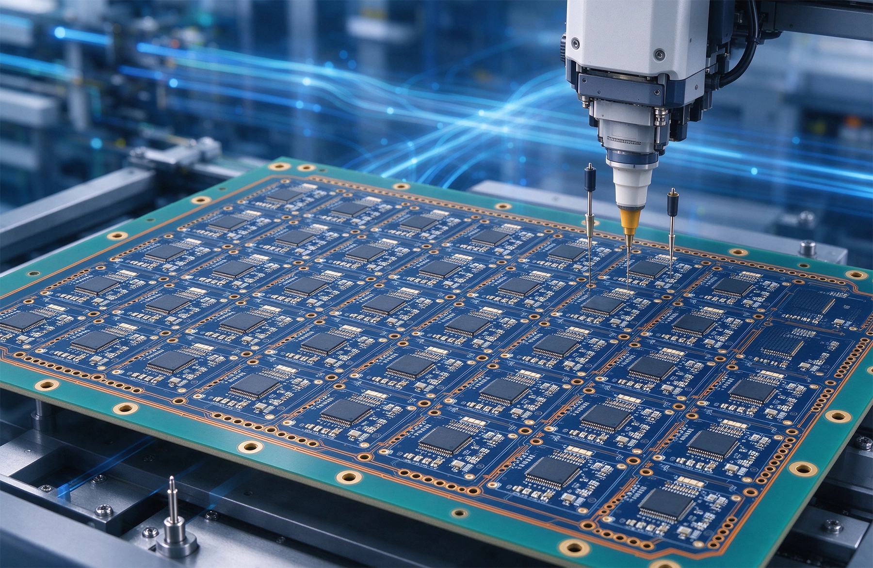
PCB assembly pricing from contract manufacturers is structured around panel utilization. A panel pass through the SMT line incurs a fixed setup cost regardless of how many functional boards are on it. If your panel holds six boards and the next design holds twenty, the per-board setup component of the cost drops dramatically for the denser panel. This is not theory; it is the fundamental basis on which assembly quotes are built.
Beyond setup amortization, panel density affects handling efficiency throughout the assembly process. A panel with well-designed fiducial placement and adequate rail clearance moves through the printer, placer, and reflow oven with fewer jams and less operator intervention. Each interruption in the line translates directly into labor cost that gets distributed across every board on the panel. Dense, well-organized panels reduce touch labor per unit and improve first-pass yield, both of which show up in your final unit price.
There is also a volume consideration that many teams overlook. Assembly shops price based on the total number of panels they need to run, not the total number of boards. If your design requires a panel density that forces the CM to run three additional panels to meet your quantity, those extra panel runs are not free. They are charged to you. Understanding this pricing structure is essential to panelization conversations with your manufacturer.
Standard PCB panel sizes exist for good reason. The most common formats in the industry are 100mm by 100mm, 150mm by 150mm, 180mm by 230mm, and 330mm by 250mm. These dimensions represent the sweet spot between usable circuit area and the physical constraints of standard SMT equipment: stencil printer beds, feeder widths, conveyor widths, and reflow oven dimensions. Designing your panel around a standard size costs nothing extra. Designing around a non-standard size invites non-standard pricing.
Before committing to a panel size, consult with your CM. Their equipment may have specific preferences or constraints that are not documented in general capability datasheets. Some manufacturers have optimized their line for specific panel dimensions and offer better pricing or faster lead times for designs that match those dimensions. A quick conversation with their engineering team before finalizing your panelization can reveal opportunities that are not visible from the outside.
The goal is to maximize the number of functional units per panel while maintaining adequate margins for the assembly process. A panel that is too densely packed risks depaneling damage, insufficient adhesive cure clearance between units, or stencil printing defects at the panel edges. A panel that wastes space with oversized rails or unnecessary routing tabs is simply leaving money on the table. The optimal density is specific to your board size, your CM's equipment, and the specific depaneling method you choose.
The method used to separate finished boards from the panel is one of the most consequential panelization choices. The two primary options are routing, where aCNC machine cuts along the periphery of each unit, and scoring, where partial V-shaped grooves are routed into the panel material along the separation lines, allowing boards to be snapped apart by hand or with a depaneling press.
Scoring is generally the lower-cost option. It requires less CNC time, produces cleaner board edges in many cases, and eliminates the need for routing bits, which wear out and add process cost. For high-volume production runs, scoring is often the preferred method because it scales linearly with panel count without significant per-panel overhead. However, scoring imposes geometric constraints: it works best when all boards on the panel are rectangular and arranged in a simple grid. Complex board shapes or designs with internal cutouts often cannot be effectively scored and require routing instead.
Routing offers more flexibility for non-rectangular board outlines and allows for more complex panelization schemes, including tab-routing where units are connected by small tabs rather than separated by full cuts. Tab routing can accommodate circular, irregular, or unusually shaped boards that would be impossible to score effectively. The trade-off is higher per-panel processing cost and slightly longer lead times. For prototypes and low-to-medium volume runs, routing adds up, and many teams find that investing in a panelization scheme that enables scoring pays for itself within the first few production batches.
There is a hybrid approach worth knowing about: routed mouse bites. This technique uses a series of small, closely spaced routed holes along the separation line, creating a perforated connection between units. Mouse bites are stronger than scored tabs and can be used for boards with moderate complexity while retaining some of the cost advantages of a scoring-style separation. Your CM's process engineering team can advise on which approach is most suitable for your specific board geometry.
The panel rails are the borders of the manufacturing panel that provide structural support during assembly processing and grip points for automated handling equipment. They are not throwaway space; they are functional real estate that must be designed with specific clearances in mind.
Standard SMT tooling requires a minimum of 3mm to 5mm of clear rail space from the nearest pad or component to the panel edge. Boards placed too close to the panel edge can experience uneven paste release during stencil printing, component placement errors due to insufficient fiducial clearance, or warping during reflow because of unbalanced copper distribution near the edge. All of these issues increase defect rates and, ultimately, cost per good unit.
Fiducial marks are another rail consideration. Most assembly processes require global fiducials on the panel rails to calibrate the pick-and-place vision system, plus local fiducials on individual boards for fine-alignment correction. Your panelization design must allocate rail space for global fiducials that are visible and unobstructed throughout the assembly process. Boards that consume all available rail space and leave no room for tooling features force the CM to place global fiducials on the functional board area, which wastes usable circuitry and may conflict with component placement.
A well-designed rail includes tooling holes in the corners for automated panel handling, global fiducial marks positioned symmetrically for consistent optical recognition, and adequate clearance around all board edges. Some manufacturers provide panelization design files or templates that specify their exact clearance requirements. Using these templates eliminates back-and-forth with the CM during design review and ensures your panel is ready for production without revision.
Beyond simply filling a standard panel with your boards, there are several techniques experienced design teams use to maximize utilization and minimize cost.
Panel utilization ratios matter more than raw board count. A panel with 95 percent of its area occupied by functional boards is far more efficient than one with 60 percent utilization, even if both panels contain the same number of units. The difference is in the handling efficiency and material waste. When evaluating a CM quote, ask about the utilization ratio they are planning for your design. If it is below 80 percent, it is worth exploring whether a different board arrangement or panel size could improve it.
Symmetry is a practical optimization that is easy to overlook. Panels with symmetric board arrangements are easier for CMs to process because the handling and depaneling equipment can be programmed more consistently. Asymmetric arrangements, where boards are staggered or oriented differently, may offer marginally better raw utilization but introduce process complexity that offsets the gain. If your board dimensions allow rotation by 90 degrees on the panel, this is a simple way to improve fit without any cost in board functionality.
Multi-up panels are worth considering for lower-volume production. Rather than designing a single board and then panelizing it, you can design the panel itself as a multi-up unit that contains the full production quantity within each panel. This approach, sometimes called "panel array" or "panel-build" design, allows for very high utilization and can dramatically reduce unit cost for smaller production quantities. The trade-off is that the individual boards in a multi-up panel must be identical, which limits this approach to products with no per-board variation.
The most effective panelization strategy is collaborative rather than unilateral. Your CM has process knowledge that is specific to their equipment, their workforce, and their existing panelization library of common formats. Tapping into that knowledge early in the design process pays dividends that far exceed the time cost of a few email exchanges or a quick call.
When requesting a quote, provide your CM with complete panelization specifications: panel size, number of units per panel, routing or scoring method, fiducial placement, and any special clearance requirements. The more specific you are, the more accurate the quote will be. A vague panelization description leads to a quote that is full of assumptions, and those assumptions often favor the CM's convenience rather than your cost interest.
Ask your CM to review your panelization design before you release files for production. Most reputable manufacturers offer this as a standard engineering review service. They will identify clearance violations, flag areas where their process capabilities may not match your design intent, and suggest optimizations based on their experience with similar designs. This review is typically free and catches issues that would otherwise become expensive surprises during production.
Build a relationship with your CM's process engineering team specifically, not just the sales team. Salespeople are good at capturing requirements; process engineers are good at telling you whether those requirements can be met efficiently. The process engineer who reviews your first production panel will likely be the same person reviewing your tenth. Consistency in the panelization approach you use across multiple designs also helps them optimize their internal processes for your account, which can translate into preferential pricing over time.
Even experienced engineering teams make panelization mistakes that add unnecessary cost. Recognizing the most common ones helps you avoid them in your own designs.
Choosing a non-standard panel size is the most frequent error. It is tempting to size your panel to fit your board with minimal waste, but a custom panel size often comes with a premium that is not obvious in the initial quote. The CM may need to cut panels from a larger stock sheet, which adds material waste, or they may need to reconfigure their line for your non-standard format, which adds setup time. Stick to standard sizes whenever your board dimensions allow it.
Underestimating clearance requirements is another common pitfall. Designers who pack boards tightly to maximize utilization sometimes specify clearances that are too small for reliable assembly. The result is a quote that looks great until the first production run reveals a high defect rate, at which point the CM comes back with a revised quote that accounts for the rework and scrap costs they are absorbing. Adding adequate clearance margins to your panelization design from the start costs nothing and protects you from this unpleasant surprise.
Ignoring depaneling stress on sensitive components is a mistake that becomes apparent only after the boards are assembled and depaneled. Components located near the board edge, particularly BGA packages and large QFPs, can crack during depaneling if the separation process applies mechanical stress to the board. The solution is to position sensitive components away from the depaneling lines or to specify routing rather than scoring when components are close to board edges. Your CM can advise on safe component placement guidelines for the depaneling method you choose.
Panelization is one of those areas where small decisions compound into significant cost differences over the life of a product. The panel size you choose, the depaneling method you specify, the clearance margins you allocate, and the relationship you build with your CM's process team all influence the final unit cost in ways that are not always visible in a component-level bill of materials. Investing time in panelization strategy before releasing your design for production is one of the highest-return activities an engineering team can undertake.
Start with standard panel formats, maximize utilization through symmetric board arrangements, choose the depaneling method that matches your board complexity, and always engage your CM in a collaborative review before files go to production. Those four practices will eliminate most of the hidden panelization costs that appear on assembly invoices, often saving more than the engineering time invested in getting them right.
Contact us to discuss your requirements.
Customer Success Story: Solving Complex Thermal Issues in PCBASeptember/18/2026
Behind the Scenes: A Tour of Our Advanced SMT Assembly FacilityAugust/07/2026
How the Global Chip Shortage is Impacting PCB Assembly ServicesJuly/23/2026

From Gerber Files to Finished Product: The Turnkey AdvantageSeptember/14/2026
Full Turnkey Solutions: Simplifying Your Supply Chain ManagementSeptember/09/2026