Open Nav



When you partner with a contract manufacturer for your PCB assembly needs, understanding the facility where your boards are produced can provide valuable insights into quality, capabilities, and operational excellence. Today, we invite you behind the scenes of our advanced SMT assembly facility to see firsthand how precision manufacturing comes to life. From incoming component inspection to final functional testing, every step in our production process reflects our commitment to delivering reliable, high-quality assembled boards for industrial, medical, aerospace, and commercial applications.
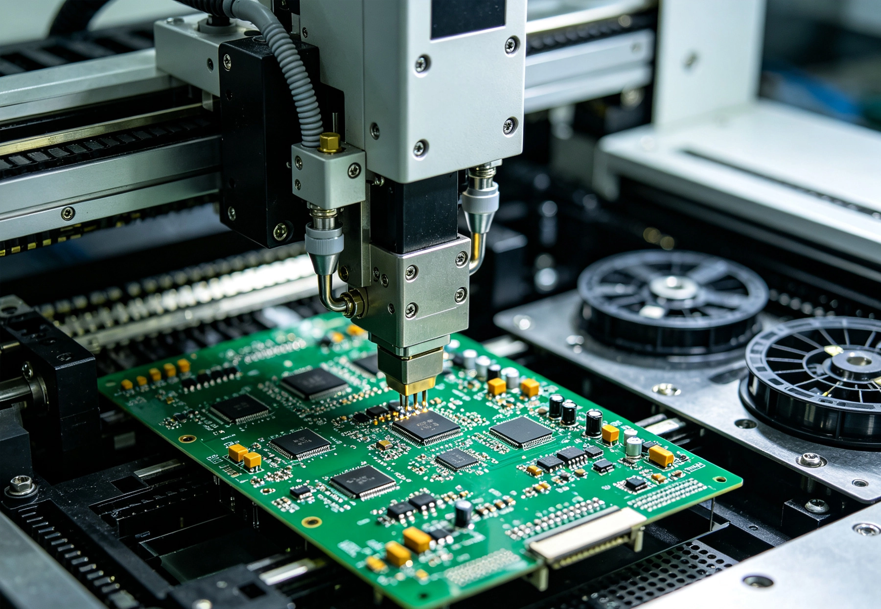
Before any board enters our production line, it begins with an environment engineered for precision. Our SMT assembly facility operates under strict clean room standards, maintaining Class 8 (ISO 14644-1) conditions throughout our primary assembly zones. Temperature is held at 23°C ± 2°C with relative humidity controlled between 40% and 60%—optimal conditions for preventing moisture-related defects and ensuring consistent solder paste behavior.
The importance of environmental control cannot be overstated. Fluctuations in temperature or humidity can dramatically affect paste viscosity, component moisture sensitivity, and finally product quality. Our facility features redundant HVAC systems with real-time monitoring, automated alerts trigger maintenance protocols before conditions drift outside acceptable parameters.
Beyond air quality, our facility incorporates comprehensive ESD (electrostatic discharge) protection. Every workstation features grounded mats, staff wear ESD-safe clothing and wrist straps, and ionizers neutralize static charges in critical assembly areas. This protects sensitive components—especially those with MOS gates and advanced semiconductor packages—from ESD damage that might not manifest until field deployment.
Every assembled board begins with solder paste application. Our facility operates a lineup ofDEK Horizon APi paste printers, equipped withadvanced vision systems and closed-loop feedback controls. The printing process might seem straightforward—apply paste to pads and place components—but achieving consistent, reliable results requires meticulous attention to parameters.
Our engineers calibrate each printer for specific board configurations, optimizing squeegee pressure, print speed, and separation distance. For boards with mixed component sizes—from fine-pitch BGAs to larger connectors—we employ dual-stage printing programs that adjust parameters automatically based on the area being processed.
Post-print inspection happens automatically. Our printers feature integrated 3D paste inspection (SPI) capability, measuring paste volume, height, and shape for every pad on every board. This catch defects at the earliest possible stage—when rework costs are minimal—rather than discovering problems after reflow.
With solder paste applied, boards move to our component placement lines. Our facility houses multiple Fuji NXT III and Panasonic NPM placement systems, capable of placing up to 45,000 components per hour while maintaining placement accuracy of ±0.03mm for fine-pitch devices. This combination of speed and precision enables us to handle everything from quick-turn prototypes to high-volume production runs.
Modern SMT assembly demands flexibility. A single production run might include 01005 passive components alongside large QFP packages, connectors, and through-hole parts. Our placement systems accommodate this diversity through modular heads that swap automatically based on component geometry. Complex boards might visit multiple placement machines, each optimized for specific component types.
Vision systems play a crucial role in placement accuracy. Top-side and bottom-side cameras verify component position relative to pad targets, correcting placement coordinates in real-time. For packages with exposed pads underneath—such as QFNs and BGAs—these systems ensure components are centered precisely over their solder paste deposits.
After component placement, boards enter our reflow ovens for solder joint formation. We operate nitrogen-inerted reflow systems that create oxygen levels below 500 ppm during processing. This inert atmosphere prevents oxidation, improves wetting, and produces more consistent solder joints—especially important for challenging finishes like OSP-coated boards or components with nickel-palladium-gold plating.
Our thermal profiling process validates every new board configuration before production. Engineers attach thermocouples to representative boards, running them through the reflow profile while recording actual temperatures at critical points. This data reveals whether components are experiencing appropriate peak temperatures and time-above-liquidus for reliable solder joint formation.
Temperature profiling also identifies potential issues before they become production problems. Cold joints might indicate insufficient peak temperature or time-above-liquidus. Tombstoning suggests uneven heating between component terminations. Both defect types can often be corrected through profile adjustments without requiring hardware changes.
Post-reflow inspection represents a critical quality checkpoint. Our assembly lines feature multiple Automated Optical Inspection (AOI) stations positioned strategically throughout the process. These systems use high-resolution cameras and sophisticated algorithms to examine every board for defects including missing components, misaligned placements, insufficient solder, excess solder, bridging, and tombstones.
Modern AOI has evolved significantly beyond simple template matching. Our systems employ rule-based inspection combined with machine learning algorithms trained on thousands of known-good and known-defective boards. This approach reduces false positives that plague older systems, preventing unnecessary rework that adds cost and cycle time.
AOI cannot catch everything—particularly defects hidden beneath components. For boards with BGA, QFN, and other bottom-terminated packages, we employ X-ray inspection as a complementary verification method. Our in-line X-ray systems provide real-time imaging of hidden solder joints, revealing voids, bridges, and insufficient connections that AOI cannot detect.
For mission-critical applications in aerospace, medical, and industrial sectors, surface inspection alone cannot provide sufficient quality assurance. Our facility offers comprehensive X-ray inspection services using automated X-ray inspection (AXI) systems capable of both 2D and 3D tomographic imaging.
AXI excels at detecting defects in ball grid arrays (BGAs) and other packages where solder joints hide beneath the component body. Voids within solder joints—voids that might lead to premature failure under thermal cycling—become clearly visible through X-ray examination. Our systems flag boards exceeding void specifications for rework before they proceed further in production.
In-circuit testing (ICT) provides another verification layer. Using bed-of-nails fixtures custom-built for each board design, ICT verifies electrical connectivity, component presence, and basic functionality before boards undergo more complex functional testing. This testing catches manufacturing defects such as opens, shorts, and incorrect component values that might escape visual inspection.
For many applications, ICT alone cannot verify that a board performs its intended function. Functional testing exercises boards under conditions simulating actual operation, verifying that analog circuits meet specification, digital logic responds correctly, and power supplies deliver appropriate voltages and currents.
Our test engineering team develops custom test programs for each customer project. These programs might include basic power-on tests, firmware upload and verification, boundary scan testing for JTAG-enabled devices, and custom functional sequences tailored to the board's end application. We maintain extensive test equipment including high-speed oscilloscopes, spectrum analyzers, power supplies, and custom test fixtures.
Burn-in testing extends quality verification for applications requiring high reliability. Boards operate at elevated temperatures while monitoring for early-life failures. This screening identifies components with latent defects that might fail in the field, allowing us to address reliability concerns before boards reach customers.
For boards destined for demanding environments—outdoor enclosures, industrial machinery, or products exposed to moisture and contaminants—we offer conformal coating and potting services. These processes add protective layers that shield circuitry from moisture, dust, chemicals, and mechanical vibration.
Our coating line features automated spray systems that apply uniform acrylic, urethane, or silicone coatings with precise thickness control. Selective coating capabilities protect connectors and test points while coating only the circuitry requiring protection. Post-application curing uses either room-temperature processes or accelerated thermal curing depending on coating material and production schedule requirements.
For extreme protection, potting and encapsulation surround entire boards in thermosetting compounds. This creates a complete barrier against environmental exposure, though it also prevents rework. Our engineers work with customers to determine appropriate protection strategies balancing reliability requirements against serviceability needs.
Modern electronics manufacturing requires comprehensive documentation and traceability systems. Our facility maintains complete records for every board produced, linking production data to specific lot codes for components, materials, and process parameters.
When quality concerns arise, this traceability enables rapid investigation. We can identify all boards produced during a specific timeframe, trace component lots back to suppliers, and verify that process parameters remained within specification. This capability proves essential for customers serving regulated industries where defect investigations and recall responses require detailed manufacturing records.
Our quality management system operates under ISO 9001:2015 certification, with additional certifications available for aerospace (AS9100D) and medical (ISO 13485) applications. Regular internal audits and third-party surveillance visits verify ongoing compliance, while our continuous improvement programs drive ongoing enhancements to processes and systems.
A visit to our SMT assembly facility reveals the extensive infrastructure, sophisticated equipment, and rigorous processes required to produce reliable electronic assemblies. From controlled environments and advanced placement systems to comprehensive inspection and testing protocols, every element contributes to the quality and reliability that industrial, medical, aerospace, and commercial customers expect.
Understanding these capabilities helps you make informed decisions about your PCB assembly requirements. Whether you need rapid prototyping, high-volume production, or specialized processes for demanding applications, our facility offers the equipment, expertise, and quality systems to support your success.
Key Terminologies You Need to Know Before Ordering PCB Assembly ServicesSeptember/07/2026
The Science of Solder Paste Printing Keys to Perfect SMT AssemblyJune/04/2026
Reducing Risk in Electronics Manufacturing with Full Turnkey ServicesAugust/15/2026
Consumer Electronics: Handling High-Density SMT AssemblySeptember/15/2026
Sustainability in PCB Assembly: Green Manufacturing Practices for the Electronics IndustryJuly/10/2026