Open Nav



Thermal management is one of the most persistent and costly challenges in printed circuit board assembly. When a product works perfectly in a climate-controlled lab but fails repeatedly in the field under real-world operating conditions, heat is almost always the culprit. Field returns, warranty claims, and reputation damage follow. For one industrial power electronics manufacturer, this scenario became a recurring nightmare — until a targeted engagement with a China-based PCBA partner revealed root causes that had gone undetected for years and delivered a solution that cut thermal failure rates by over 90%.
This article walks through that real-world case study — the diagnostic process, the engineering decisions, and the results — as a practical guide for engineers and product managers facing similar challenges.
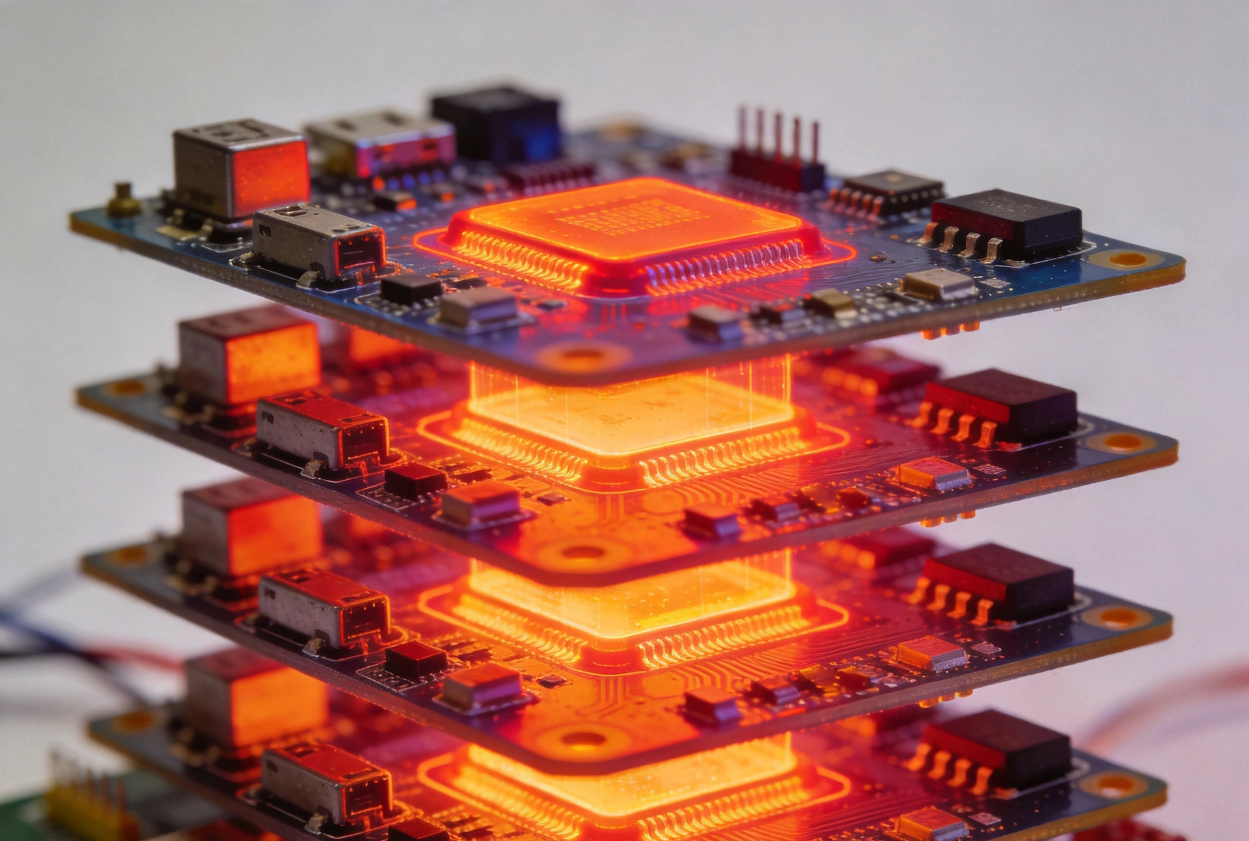
The customer was a European manufacturer of industrial motor drive controllers — compact, high-power units deployed in factory automation systems across Southeast Asia and the Middle East. Their products operated in environments where ambient temperatures routinely exceeded 45°C, with internal enclosure temperatures reaching 85°C or higher during peak load conditions.
The symptoms were consistent and troubling:
The customer had spent over 18 months trying to solve the problem internally. They had replaced components with higher temperature-rated alternatives, added external heatsinks, and modified the enclosure design. None of these changes eliminated the failures. The pattern suggested a systemic issue that individual component swaps could not address.
When the customer engaged a specialized China PCBA manufacturer with in-house thermal engineering capabilities, the investigation took a fundamentally different approach.
The first step was to stop guessing and start measuring. The engineering team installed thermocouples at 24 key points across a production unit — on the PCB surface, at component leads, inside the enclosure, and at the enclosure exterior. Data loggers recorded temperature at 1-second intervals during a simulated full operating cycle.
What the baseline revealed was alarming but clarifying:
The datasheet limits that had been consulted during component selection had been applied correctly — but they had been applied without accounting for the thermal interaction between components in a densely packed enclosure. Individual component ratings told only part of the story.
Thermal problems in PCBA rarely have a single root cause. In this case, the investigation identified three distinct but interconnected issues, each requiring its own solution.
The original PCB was a standard 4-layer board with 1oz copper on all layers and standard FR-4 material (Tg 130°C). While this specification was adequate for electrical performance, it created a thermal bottleneck. Heat generated by the MOSFETs on the top layer had to conduct vertically through the dielectric layers to reach the bottom thermal pad and the enclosure base — but the thermal conductivity of standard FR-4 is extremely low, approximately 0.3 W/mK.
Thermal simulation showed that switching to a board with 2oz copper on the power planes and adding a metal-core thermal via array under the MOSFET footprint could reduce the thermal resistance from junction to ambient by nearly 40%.
The MOSFETs used a D2PAK package with a large thermal pad on the bottom. During assembly, the solder paste stencil aperture had been designed with a 60% coverage ratio — a compromise made years earlier to prevent solder bridging. At high thermal loads, the insufficient solder bond created a thermal interface resistance that further trapped heat at the package junction.
Cross-section analysis of field-returned units confirmed voiding rates above 30% in the thermal pad solder joint — well above the IPC-7095 Class 3 recommended maximum of 25%.
The PCB mounted to the enclosure base through a thermal pad interface. The material selected — a standard silicone thermal pad with 1.5 W/mK conductivity — was insufficient to transfer heat from the board to the aluminum enclosure at the required rate. The contact pressure was also inconsistent, as the mounting screw torque specification had not been validated against actual thermal performance.
With the root causes identified, the engineering team implemented a phased remediation plan.
The board stackup was modified to 4 layers with 2oz copper on the two inner power planes, targeted thermal via arrays under all major heat-generating components, and a dedicated thermal spreading plane on Layer 2 with direct thermal vias to the bottom side. The total board thickness was held constant to maintain compatibility with the existing enclosure mounting points.
The solder paste stencil aperture for the MOSFET thermal pad was redesigned to achieve 85% coverage — a compromise between voiding risk and bridging risk, validated through DOE (design of experiments) testing. A no-clean SAC305 paste with superior thermal fatigue resistance was selected over the previous SnPb formulation. Reflow profile parameters were re-optimized to ensure consistent solder joint formation across the board.
The silicone thermal pad was replaced with a graphite thermal interface sheet rated at 6 W/mK conductivity. Mounting screw torque was specified and validated at 0.5 Nm with a calibrated torque driver. A thermal interface material thickness tolerance of ±0.1mm was established and inspected at incoming quality control.
Three small ventilation slots were laser-cut into the enclosure base plate, positioned to allow natural convection airflow across the lower face of the board. Computational fluid dynamics (CFD) simulation was used to optimize slot size and position — too large would compromise EMC shielding; too small would provide insufficient airflow. The final design used 2mm-wide slots with EMI gaskets to maintain EMC compliance.
Design changes mean nothing without validation. The revised design underwent a comprehensive test protocol:
All test vehicles passed without failure. Cross-section analysis of solder joints from the HTOL test showed voiding rates below 15% — well within IPC Class 3 limits and a significant improvement over the 30%+ rates observed in field returns.
Following the production rollout of the redesigned assemblies, the customer tracked field performance over a 12-month observation period. The results were unambiguous:
The return on investment for the redesign program was achieved within the first three months of production — a compelling outcome that the customer's procurement team found easy to justify.
Several insights from this case study apply broadly to thermal management challenges in high-power PCBA applications.
Every component datasheet provides a thermal resistance junction-to-case or junction-to-ambient specification. These numbers are accurate under the specific test conditions described in the datasheet — conditions that rarely match the actual operating environment inside your enclosure. Always apply appropriate derating factors and verify thermal performance empirically in your specific system configuration.
A single component operating in isolation may be well within its limits. Add six neighboring components all generating heat in a confined space, and the temperature at each location rises significantly. Thermal simulation tools and empirical measurement with thermocouples or infrared imaging are essential for identifying these interactions before they cause field failures.
Voiding in thermal pad solder joints does not just weaken the mechanical bond — it dramatically increases thermal resistance, trapping heat at the component junction. For packages with exposed thermal pads (QFN, D2PAK, TQFN), stencil design and reflow profile optimization are as much thermal engineering decisions as they are assembly process decisions.
The most effective thermal improvements in this case were not dramatic — a different PCB stackup, a modified stencil aperture, a different thermal interface sheet. None of these changes required a new enclosure or a new component lineup. Often, the biggest gains come from a combination of modest, well-targeted changes rather than wholesale redesigns.
The customer had been unable to reproduce the failures in-house because the failures were thermally driven by the specific combination of high ambient temperature, high load, and extended operating time that only occurred in real field conditions. When troubleshooting chronic thermal issues, always seek actual field return units and failure data. Temperature logging from deployed units provides invaluable insight that accelerated life testing alone cannot fully replicate.
Thermal management in PCBA is a systems engineering challenge, not a component selection exercise. The most effective solutions emerge from a combination of empirical measurement, root cause analysis across multiple dimensions, and targeted design changes backed by validation data. In this case, a thorough thermal audit revealed issues that had gone undetected for over 18 months — and the corrected design delivered a 93% reduction in failure rate with a payback period measured in weeks rather than years.
For manufacturers experiencing unexplained field failures in high-power or high-temperature applications, a structured thermal investigation — with thermocouple measurement, cross-section analysis, and thermal simulation — is almost always worth the investment. The cost of the investigation is small compared to the cumulative cost of field failures, warranty处置, and reputational damage.
Working with a PCBA partner that has in-house thermal engineering capability — including thermal simulation tools, cross-section analysis, and accelerated life testing — can be the difference between repeatedly patching a problem and actually solving it.
Signs pointing to thermal causes include failures that cluster in high-temperature climates or during peak load conditions, inconsistent failure modes across different units, a lack of reproducible failures under standard in-house test conditions, and failure analysis reports showing component degradation patterns consistent with overheating (discolored solder joints, cracked die attach, swollen capacitors). Thermal logging of deployed units in their actual operating environment is the most reliable diagnostic method.
Adding thermocouples to production units and operating them under monitored real-world conditions — or retrieving field-returned units for cross-section analysis — provides the highest-value diagnostic information at the lowest cost. This empirical data tells you exactly where heat is accumulating and which components are at risk, guiding subsequent design changes rather than requiring expensive redesigns based on guesswork.
Thermal simulation tools (FEA and CFD) are excellent for exploring design alternatives quickly and for identifying thermal bottlenecks during the design phase. However, they require accurate component power dissipation models and material property data to produce reliable results. Physical testing — thermocouple measurement, infrared thermography, and accelerated life testing — remains essential for validating simulation predictions and catching issues that models do not capture, such as contact resistance variations or unexpected airflow patterns.
The cost varies widely depending on the scope of changes required. In this case study, the PCB stackup and process changes added approximately $1.80 per board — a modest increase that was far outweighed by the reduction in field failure costs. The key is to pursue targeted changes identified through root cause analysis rather than a blanket redesign. An engineering engagement focused on thermal investigation and targeted redesign typically costs between $3,000 and $15,000, depending on complexity — a fraction of the cost of sustained field failures in high-volume production.
Solder paste choice affects thermal management in several ways. Lead-free SAC alloys (SAC305, SAC405) offer better thermal fatigue resistance than tin-lead solders at elevated temperatures, but they are also more susceptible to voiding in large thermal pad areas. No-clean paste formulations generally produce lower voiding rates than water-wash formulations due to their flux chemistry. For high-thermal-load applications, selecting a paste specifically formulated for thermal pad applications — with appropriate stencil aperture design — can reduce voiding rates from 30%+ to below 15%, with a measurable impact on junction temperature.
Thermal via arrays significantly improve heat transfer from the component to the board's internal copper planes and ultimately to the enclosure or heatsink. However, improper via design can introduce manufacturing defects. Vias must be properly tented or plugged on the surface to prevent solder wicking into the via barrel during reflow, which creates voids under the thermal pad. The via diameter, pitch, and plating thickness must be optimized to balance thermal performance with manufacturing yield. A typical thermal via array uses 0.3–0.4mm vias on 0.8–1.0mm pitch with electroless nickel gold plating.
Common SMT Defects and How to Prevent Them in Your DesignJuly/03/2026

Consumer Electronics: Handling High-Density SMT AssemblySeptember/15/2026

Overcoming Minimum Order Quantity (MOQ) Challenges in PCBAAugust/14/2026
Medical PCBA: Meeting Strict Regulatory Standards in AssemblySeptember/01/2026

From Gerber Files to Finished Product: The Turnkey AdvantageSeptember/14/2026