Open Nav



Component spacing represents one of the most critical design considerations in printed circuit board (PCB) assembly, directly affecting manufacturing yield, assembly efficiency, and overall production costs. Proper spacing between components ensures reliable soldering, facilitates automated assembly processes, minimizes the risk of manufacturing defects, and enables efficient inspection and rework procedures. This comprehensive guide explores the principles, guidelines, and strategies for optimizing component spacing to achieve efficient PCB assembly while maintaining electrical performance and manufacturing reliability.
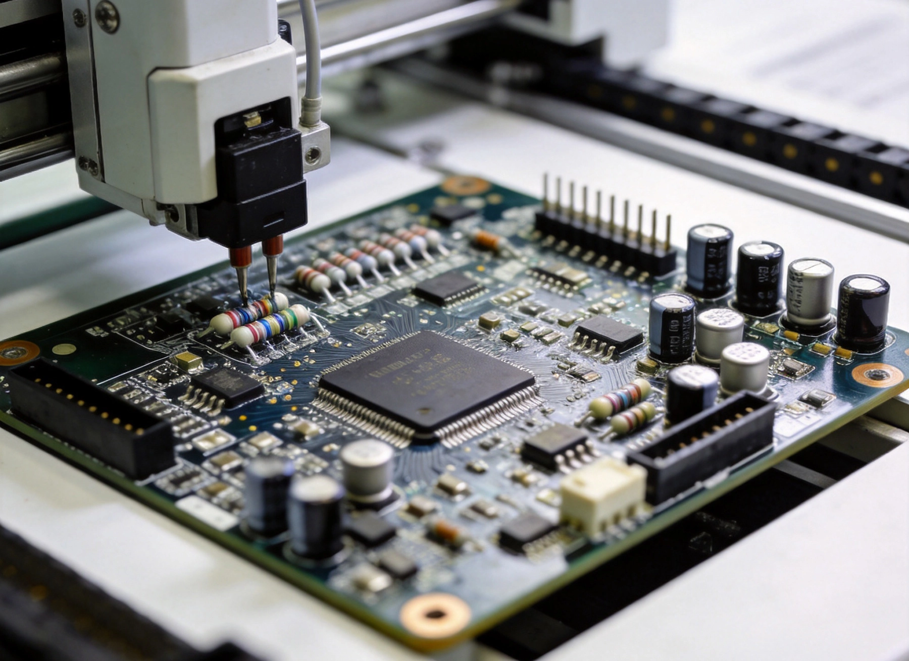
The fundamental purpose of component spacing extends beyond simply fitting components onto a board. Adequate spacing accommodates manufacturing tolerances, thermal expansion differences, and mechanical stress while enabling efficient assembly processes. Component spacing must account for placement machine accuracy, solder paste printing variations, reflow soldering characteristics, inspection requirements, and potential rework operations. Each of these factors contributes to determining appropriate minimum spacing requirements for different component types and board configurations.
The relationship between component spacing and manufacturing yield follows a clear correlation: insufficient spacing increases defect rates dramatically, while excessive spacing wastes valuable board area without providing proportional benefits. Finding the optimal balance requires understanding the specific manufacturing capabilities, assembly equipment, and quality requirements for each production environment. What works for low-volume, high-reliability military applications may be inappropriate for high-volume consumer electronics, and vice versa.
Component spacing also impacts electrical performance through coupling effects, electromagnetic interference, and signal integrity considerations. While this guide primarily focuses on manufacturing aspects, designers must balance spacing requirements for efficient assembly with electrical design requirements, particularly for high-speed or sensitive analog circuits. In many cases, electrical and manufacturing spacing requirements align, but designers must remain aware of potential conflicts and develop appropriate compromise solutions.
Surface-mount technology (SMT) components represent the majority of modern PCB assemblies, and their spacing requirements depend heavily on component body size, lead pitch, and termination type. For small components such as 0402 (1.0mm × 0.5mm) and 0201 (0.6mm × 0.3mm) chip resistors and capacitors, minimum spacing typically ranges from 0.15mm to 0.25mm depending on the assembly process capabilities. These tiny components present significant assembly challenges due to their small size and susceptibility to tombstoning and bridging defects, making adequate spacing crucial for reliable manufacturing.
Larger SMT components including 0603, 0805, and 1206 packages generally require minimum spacing of 0.25mm to 0.5mm to accommodate solder paste printing tolerances and placement machine accuracy. Fine-pitch components such as quad flat packages (QFP) and ball grid arrays (BGA) demand even more careful spacing considerations. For fine-pitch QFPs with pitches down to 0.5mm or 0.4mm, spacing to adjacent components typically should not be less than the component pitch to prevent solder bridging between leads. BGA components require clearance for both the component body and any peripheral routing or decoupling capacitors, with minimum spacing of 0.5mm to 1.0mm recommended depending on ball pitch and assembly equipment capabilities.
Through-hole components present different spacing challenges. While their larger size generally makes spacing less critical than with tiny SMT components, adequate spacing remains essential for wave soldering processes, manual insertion operations, and proper fluxing. For dual in-line packages (DIP), spacing between adjacent DIPs should typically be at least 0.5mm to 1.0mm to accommodate lead bending variations and wave soldering requirements. Radial leaded components such as electrolytic capacitors and transformers require clearance for their larger body sizes and lead bending allowances, with spacing typically in the 1mm to 2mm range depending on component dimensions.
The chosen assembly process significantly influences appropriate spacing guidelines. Reflow soldering, the most common SMT assembly process, accommodates tighter spacing compared to wave soldering or selective soldering processes. During reflow, solder paste deposits remain localized around component pads, enabling closer component placement as long as paste printing accuracy meets requirements. However, reflow soldering introduces challenges with tombstoning on small passives when thermal gradients cause uneven heating across the component body, making consistent spacing critical for uniform thermal distribution.
Wave soldering, primarily used for through-hole components and mixed-technology boards, demands larger component clearances due to the solder wave's contact characteristics. Components must be positioned with sufficient spacing to prevent the solder wave from wicking under adjacent components and creating bridges or short circuits. Additionally, wave soldering requires specific component orientation relative to the wave direction to ensure reliable solder fillet formation, creating additional spacing constraints based on wave soldering equipment specifications and process parameters.
Selective soldering processes, which apply solder only to specific locations rather than across the entire board, enable tighter spacing for components that undergo selective soldering. However, selective soldering introduces its own spacing considerations related to nozzle clearance, flux application, and solder flow characteristics. Designers must understand their specific selective soldering equipment capabilities and process parameters to establish appropriate spacing guidelines for components undergoing selective soldering processes.
Effective DFM practices incorporate component spacing guidelines directly into the design process, preventing spacing-related manufacturing issues before they occur. The foundation of DFM spacing rules involves establishing minimum spacing requirements based on specific manufacturing capabilities rather than generic industry guidelines. Each assembly facility maintains its own capabilities matrix documenting minimum achievable spacing for different component types, board sizes, and process variations. Designers should work with their manufacturing partners to understand these capabilities and incorporate them into design rules from the project outset.
Design rule checking (DRC) tools in CAD software provide automated verification of component spacing against established guidelines. Setting appropriate DRC parameters prevents spacing violations before designs reach manufacturing, saving time and cost by eliminating design iterations. However, designers must configure DRC rules accurately based on actual manufacturing capabilities rather than default settings that may be either too restrictive or too permissive for their specific assembly process.
Component placement software, often integrated into CAD systems or used as standalone tools during panelization, provides additional spacing verification capabilities. These tools simulate the actual component placement process, identifying potential interference issues that might not be caught by standard DRC checks. Particularly useful for high-density designs with components packed tightly together, placement verification tools help identify spacing issues before designs progress to manufacturing, reducing the risk of costly re-spins.
Thermal management requirements significantly impact component spacing decisions. Heat-generating components such as power regulators, processors, and power transistors require adequate spacing from heat-sensitive components to prevent thermal damage. The thermal relationship between components depends not only on physical distance but also on thermal conductivity of PCB materials, presence of thermal vias, and airflow characteristics during operation and assembly. Designers must consider both steady-state operating temperatures and reflow soldering thermal profiles when establishing spacing between thermally sensitive components.
Components with different coefficients of thermal expansion (CTE) require spacing accommodations for dimensional changes during thermal cycling. Large BGA packages, particularly those on organic substrates, expand significantly during reflow soldering, potentially stressing adjacent components or solder joints if spacing is insufficient. Similarly, components with plastic bodies expand at different rates than ceramic components, creating potential spacing conflicts during temperature excursions. Designers working with mixed-material assemblies must account for these CTE differences when establishing spacing guidelines.
Reflow thermal profiles affect component spacing requirements through differential heating rates. Components with large thermal mass heat more slowly than small components during reflow, creating temperature gradients across the board. These gradients can cause tombstoning on small components when one end heats faster than the other, or can cause shifting of components if thermal expansion forces overcome solder paste tack. Adequate spacing helps mitigate these thermal effects by providing clearance for component movement and ensuring uniform thermal exposure during the reflow process.
High-density PCB designs demand innovative spacing optimization strategies to maximize component density while maintaining manufacturability. Component stacking technologies enable placing smaller components underneath larger components, effectively utilizing the vertical dimension for spacing relief. However, stacking introduces assembly sequence challenges and potential rework complications, requiring careful process planning and design consideration. Stacking typically works best when the bottom-side component requires no rework after top-side component assembly, or when assembly processes accommodate top-side component removal if bottom-side rework becomes necessary.
Component selection represents another powerful strategy for optimizing spacing in high-density designs. Choosing components with smaller footprints, optimized termination geometries, or innovative package styles enables tighter spacing without compromising reliability. For example, chip-scale packages (CSP) and wafer-level chip-scale packages (WLCSP) provide significantly reduced footprints compared to traditional QFP or BGA packages, enabling denser packing while maintaining assembly reliability. However, these advanced packages often require specialized assembly capabilities, so designers must verify that their manufacturing partners support the chosen component technologies.
Panelization strategies affect component spacing efficiency through inter-panel and intra-panel optimization. Efficient panel layouts maximize board count per panel while maintaining adequate spacing between components and panel edges for handling, routing, and assembly processes. Intra-panel spacing optimization involves arranging components on individual boards to minimize wasted space while respecting spacing requirements. Sophisticated panelization software automatically evaluates multiple layout configurations, identifying the most efficient arrangement that meets all spacing, handling, and manufacturing requirements.
Component spacing directly impacts inspection and rework capabilities, crucial factors for maintaining high manufacturing yield and quality. Automated optical inspection (AOI) systems require adequate component spacing to achieve reliable defect detection. Too-tight spacing can cause shadowing effects where components block the camera's view of adjacent solder joints or component bodies, preventing effective inspection. Similarly, X-ray inspection capabilities depend on spacing to achieve clear images of hidden solder joints beneath components like BGAs, with inadequate spacing potentially causing image artifacts or interpretation challenges.
Manual rework operations demand significantly more spacing than automated assembly processes. Technicians need adequate clearance to access components with soldering irons, hot air rework tools, or tweezers without disturbing adjacent components. Rework considerations become particularly important for components with high rework probability, such as BGAs, large fine-pitch QFPs, or connectors. Designers working with high-reliability applications where rework is anticipated should incorporate enhanced spacing allowances for these components to facilitate efficient, reliable rework operations without affecting surrounding assemblies.
Test point accessibility provides another spacing consideration for manufacturing test operations. Test probes require clearance from nearby components to avoid accidental contact or mechanical interference during testing. In-circuit test (ICT) and flying probe test systems each have specific spacing requirements based on probe size, access angle, and deflection characteristics. Designers must ensure adequate spacing between test points and nearby components, or consider alternative test strategies such as boundary scan (JTAG) for components with spacing constraints that preclude physical probe access.
Industry standards provide valuable guidance for establishing appropriate component spacing requirements. The IPC (Association Connecting Electronics Industries) publishes comprehensive guidelines including IPC-7351 for land pattern standards, which includes spacing recommendations based on component types and manufacturing capabilities. These standards represent industry consensus derived from extensive manufacturing experience across diverse applications and serve as excellent starting points for establishing spacing guidelines. However, designers should adapt standard guidelines to their specific manufacturing capabilities rather than applying them rigidly without considering actual process capabilities.
Component manufacturer datasheets often include recommended spacing guidelines based on their specific package characteristics and assembly experience. These recommendations typically represent minimum spacing for reliable assembly rather than optimal spacing for efficient manufacturing. Designers should treat manufacturer recommendations as baseline requirements and consider incorporating additional spacing margins based on their specific manufacturing environment and quality requirements.
Design rule documentation, maintained internally by design organizations, captures spacing lessons learned from previous designs and manufacturing experiences. This institutional knowledge represents a valuable resource for optimizing spacing on new designs. Documenting both successful spacing choices and manufacturing issues attributed to inadequate spacing creates a knowledge base that continuously improves design practices over time. Organizations implementing systematic design review processes should incorporate spacing-specific reviews to capture and disseminate lessons learned across design teams.
Component spacing decisions directly affect manufacturing costs through yield, board utilization, and assembly efficiency impacts. Insufficient spacing increases defect rates, particularly for solder bridges, tombstoning, and assembly machine placement errors. These defects drive up manufacturing costs through increased rework, scrap, and potential field failures. The cost of a single spacing-related defect cascade through the entire manufacturing process, from additional inspection time to rework labor to potential field returns, making spacing optimization a high-value design activity.
Excessive spacing wastes board area without providing proportional manufacturing benefits, increasing material costs and potentially reducing functionality density. For consumer electronics applications where board space represents a significant cost driver, oversizing spacing unnecessarily reduces product competitiveness by increasing size or reducing feature density. The optimal spacing balances manufacturing reliability with board utilization efficiency, requiring careful analysis of specific application requirements and cost structures.
Assembly machine efficiency depends on component spacing through nozzle selection, path optimization, and throughput considerations. Tight component packing may require smaller, slower nozzles that reduce throughput, or may necessitate additional pick-and-place passes that increase cycle time. Larger spacing enables use of larger, faster nozzles and more efficient placement paths, potentially reducing assembly costs through higher throughput. However, these throughput gains must be balanced against board area costs to determine the most cost-effective spacing strategy for each application.
Advancing component miniaturization continues to push spacing requirements to new limits. As component footprints shrink toward 01005 (0.4mm × 0.2mm) and beyond, traditional spacing guidelines become increasingly difficult to achieve. Emerging assembly technologies including advanced placement machines with sub-micron accuracy, improved solder paste printing systems, and enhanced inspection capabilities enable tighter spacing but require corresponding investments in equipment and process development. Designers working with the most advanced technologies must maintain close collaboration with manufacturing partners to establish realistic spacing expectations based on current capabilities.
Additive manufacturing approaches offer potential spacing relief by eliminating subtractive processes that drive traditional spacing requirements. Direct component printing technologies may eventually enable novel spacing strategies unrestricted by traditional pick-and-place limitations. However, these technologies remain in development for most commercial applications, meaning designers must continue working within the constraints of conventional assembly processes for the foreseeable future while monitoring emerging technologies for future implementation opportunities.
Automated design optimization tools increasingly incorporate spacing considerations into automated layout algorithms. Artificial intelligence and machine learning approaches enable intelligent component placement that optimizes spacing based on multiple criteria including manufacturability, electrical performance, thermal management, and cost. These tools can rapidly evaluate thousands of potential layout configurations, identifying spacing-optimized solutions that might be missed through manual design approaches. As these tools mature, they promise to streamline spacing optimization while reducing the designer burden of managing complex spacing requirements across diverse design constraints.
Optimizing component spacing requires a strategic approach that balances multiple competing requirements including manufacturability, electrical performance, thermal management, and cost. Successful spacing optimization begins with understanding specific manufacturing capabilities and constraints, then incorporating appropriate guidelines into the design process from the earliest design stages. Designers who work proactively with manufacturing partners, leverage DFM best practices, and utilize appropriate design tools achieve more efficient designs with fewer manufacturing iterations and higher overall success rates.
The fundamental principle underlying effective spacing optimization involves finding the minimum spacing that ensures reliable assembly without compromising other critical requirements. Too little spacing creates manufacturing problems and quality issues, while too much spacing wastes board area and increases costs unnecessarily. The optimal spacing provides adequate clearance for all assembly, inspection, and rework operations while maximizing board utilization efficiency and maintaining electrical performance.
As component technologies continue advancing and assembly processes become increasingly sophisticated, spacing optimization will remain an essential aspect of PCB design. Designers who stay informed about emerging technologies, maintain strong relationships with manufacturing partners, and apply systematic DFM approaches will be well-positioned to meet evolving spacing challenges while maintaining design excellence and manufacturing efficiency. Component spacing may seem like a mundane design consideration, but its impact on manufacturing yield, cost, and product reliability makes it one of the most important factors in successful PCB design and assembly.

Avoiding Tombstoning and Bridging in Your PCB LayoutJuly/30/2026

How the Global Chip Shortage is Impacting PCB Assembly ServicesJuly/23/2026
Precision SMT PCB Assembly for Wearable TechnologyJune/16/2026
X-Ray Inspection: Detecting Hidden Defects in BGA and QFN PackagesAugust/10/2026
Full Turnkey Solutions: Simplifying Your Supply Chain ManagementSeptember/09/2026