Open Nav


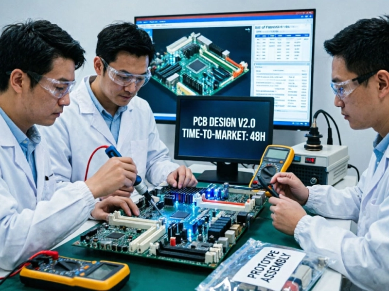
Turnkey PCB assembly transforms a design concept into a finished electronic product through a coordinated manufacturing process. From the initial bill of materials through final box build, each stage builds upon the previous one, creating an assembled product ready for deployment. Understanding this workflow helps designers, engineers, and product managers navigate manufacturing relationships and optimize products for efficient production.
The term "turnkey" reflects the comprehensive nature of these services: you provide the design and specifications, and the manufacturer handles everything else through delivery of complete, tested products. This approach eliminates coordination complexity between multiple suppliers while providing single-source accountability for quality and delivery. Whether you're developing a simple sensor module or a complex multi-board system, the fundamental workflow follows similar patterns with variations based on product complexity and requirements.
This guide walks through the complete turnkey PCB assembly process, from initial component procurement through final box build, explaining what happens at each stage and why certain steps matter for product quality and reliability.
Every successful assembly project begins before production starts. The design handoff establishes the foundation for manufacturing execution and quality assurance.
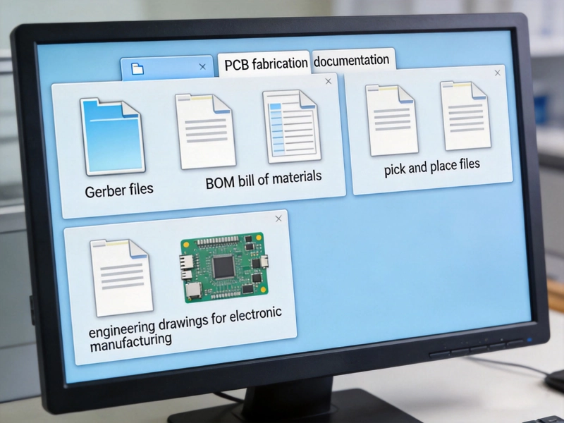
Turnkey assembly requires comprehensive documentation:
Experienced turnkey providers conduct Design for Manufacturing (DFM) reviews before production commitment:
Manufacturing Feasibility Assessment: Engineers evaluate whether the design can be manufactured reliably at scale. They identify components that are difficult to place, fine-pitch devices requiring specialized equipment, or thermal management concerns during reflow.
Component Availability Check: The BOM undergoes scrutiny for component availability, obsolescence risks, and allocation concerns. Long-lead components or parts with extended lead times may require design modifications or alternative sourcing strategies.
Cost Optimization Opportunities: DFM reviews often identify design elements that increase manufacturing cost without adding value—unnecessary fine-pitch components, overly tight tolerances achievable through relaxation, or component choices with cheaper alternatives.
Test Coverage Analysis: Engineers review test access points and controllability to ensure the design supports adequate testing. Designs without test access may require modification to enable comprehensive testing.
With approved designs, the turnkey provider initiates component procurement—the stage that most directly impacts production timelines and cost.
Professional turnkey assembly providers employ strategic procurement approaches:
Authorized Distribution Channels: Components sourced through authorized distributors carry manufacturer warranties and reduced counterfeit risks. While more expensive than grey market sources, authorized procurement protects product reliability and manufacturer liability.
Long-Lead Component Prioritization: Components with extended lead times receive procurement priority to prevent these items from gating the production schedule. Providers identify critical path components early and accelerate their procurement.
Alternative Part Identification: For components with availability concerns, procurement teams identify drop-in replacements or pin-compatible alternatives. This proactive approach prevents production delays from component unavailability.
Components undergo verification upon receipt:
Turnkey providers maintain inventory strategies that balance availability against carrying costs:
Buffer Stock: For stable products, providers may maintain component buffer inventory that enables rapid response to reorder requests without procurement lead time.
Consignment Options: Some arrangements involve customer-owned inventory held at the provider's facility, reducing provider inventory risk while providing quick-turn availability.
Component Aging Monitoring: Components approaching age limits or moisture sensitivity exposure receive priority allocation to prevent shelf-life expiration.
While assembly receives primary attention in turnkey services, PCB fabrication establishes the foundation upon which assembly quality depends.
PCB fabrication transforms raw laminate materials into manufactured boards:
Material Preparation: Laminate sheets cut to panel size undergo cleaning and surface preparation for copper bonding.
Imaging: Photoresist-coated panels expose to UV light through film artwork, transferring the Gerber-defined pattern to the copper surface.
Plating and Etching: Copper plating builds trace thickness, followed by chemical etching that removes unwanted copper, leaving the designed trace pattern.
Lamination (Multi-Layer Boards): Inner layers stack with prepreg bonding material and outer layers, then consolidate under heat and pressure in a lamination press.
Drilling and Plating: Holes drilled through the board receive conductive plating that creates electrical connections between layers.
Surface Finish: Surface finishes—HASL, ENIG, OSP, or immersion silver—protect exposed copper and provide solderability.
Solder Mask and Silkscreen: Solder mask covers non-component areas while silkscreen prints component designators, logos, and other markings.
Fabrication quality verification includes:
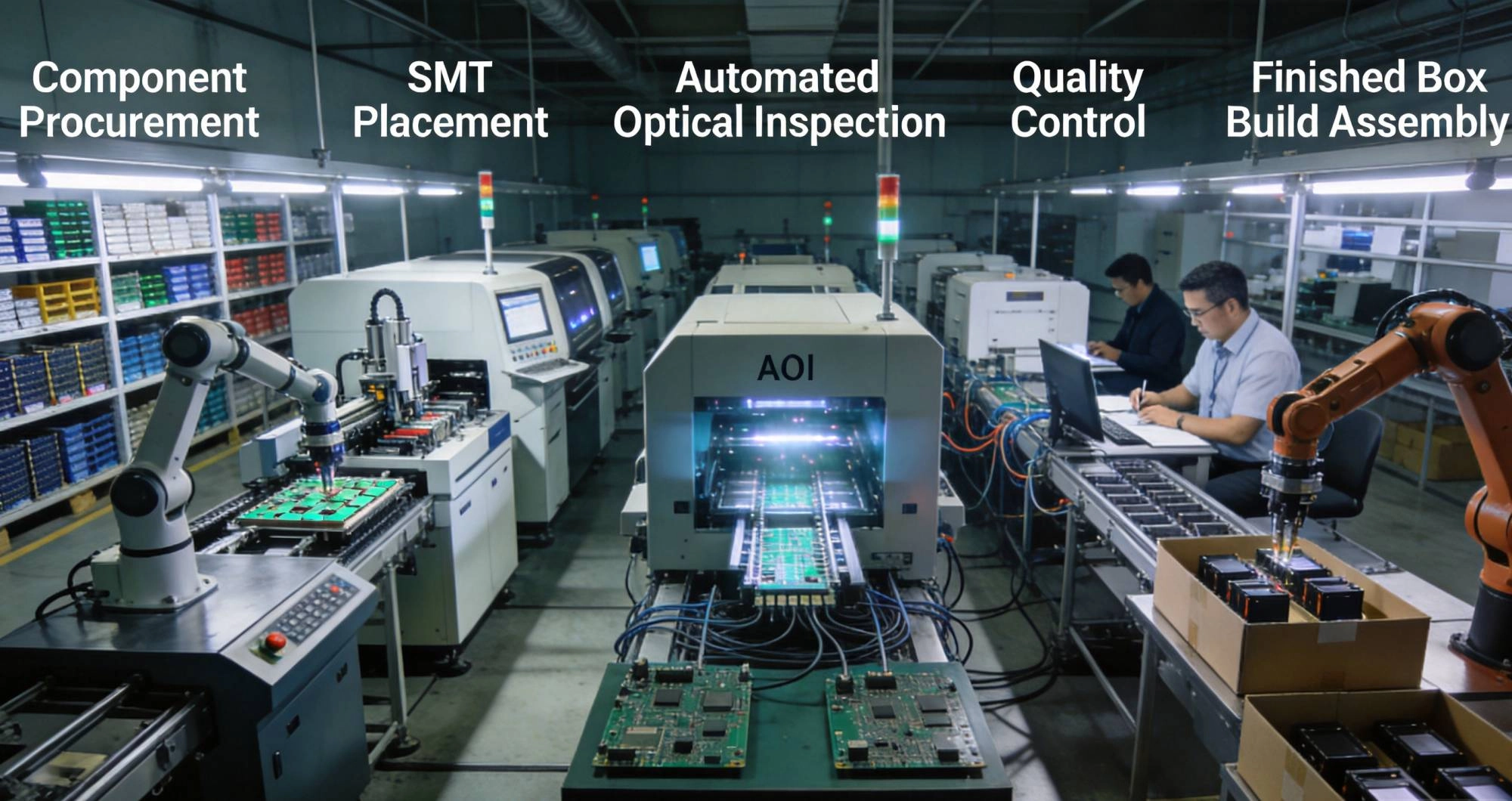
With fabricated boards and verified components ready, assembly transforms individual parts into populated circuit assemblies.
Before component placement, solder paste applies to board pads:
Stencil Preparation: Laser-cut stencils match board pad geometry, controlling paste volume deposition precisely.
Paste Printing: Automated stencil printers deposit solder paste in exact locations across the panel. Printer alignment systems ensure paste registers perfectly with pad patterns.
Inspection: Automated Paste Inspection (API) systems verify paste volume and placement before components enter the equation.
Modern assembly uses automated placement systems:
Pick and Place Machines: High-speed placement heads collect components from feeders and place them precisely on paste-covered pads. Modern machines place 40,000+ components per hour with placement accuracy of ±0.025mm.
Component Verification: Vision systems confirm component presence and orientation immediately after placement, catching missing or misaligned parts before reflow.
Fine Pitch Handling: BGA, QFN, and 0201/01005 components require specialized equipment and process parameters beyond standard SMT placement.
Placed components transfer to reflow ovens for soldering:
Thermal Profile: The reflow profile—temperature versus time—governs solder joint formation. Profiles include preheat, soak, reflow, and cooling zones optimized for specific solder alloys and board characteristics.
Lead-Free Considerations: RoHS-compliant products use lead-free solders requiring higher peak temperatures (typically 245-260°C versus 225°C for tin-lead). These elevated temperatures require thermal management for temperature-sensitive components.
Controlled Cooling: Controlled cooling rates prevent thermal shock and ensure proper grain structure in solder joints.
Products with through-hole components require additional processing:
Wave Soldering: For mixed-technology boards, wave soldering selectively solders through-hole leads after SMT reflow.
Hand Assembly: Some through-hole components—connectors, transformers, or large electrolytic capacitors—may require hand soldering for thermal management or physical access reasons.
Press-Fit Technology: Some applications use press-fit pins that cold-weld into plated holes without solder, eliminating thermal stress from wave soldering.
Assembly completion begins inspection and testing that verifies product functionality before shipment.
Multiple inspection modalities catch defects:
Automated Optical Inspection (AOI): High-resolution cameras image assembled boards, comparing against golden board references to identify component placement issues, solder defects, and marking errors. AOI catches 80-90% of assembly defects.
X-Ray Inspection: For hidden solder joints—BGA, QFN, and other bottom-terminated components—X-ray imaging reveals solder joint quality beneath the component body where optical inspection cannot reach.
SPI and AOI Integration: Combining Solder Paste Inspection with AOI creates closed-loop process control that identifies both paste deposition issues and component placement problems.
Electrical verification ensures functional correctness:
In-Circuit Testing (ICT): Bed-of-nails fixtures make contact with test points on the board, verifying component presence, values, and circuit connectivity. ICT typically achieves >95% defect coverage for detectable defects.
Flying Probe Testing: For low-volume or complex boards where fixture costs are prohibitive, flying probe systems move measurement contacts to test points without dedicated fixtures.
Functional Testing: Power application and functional verification tests the board as it would operate in the final product, exercising circuits and verifying performance against specifications.
Inspection findings trigger analysis:
Root Cause Analysis: Systematic investigation determines why defects occurred—whether component issues, process variation, or design problems.
Rework Procedures: Defects that are repairable undergo controlled rework: component replacement, solder bridge removal, or solder joint reformation using specialized rework equipment.
Process Adjustments: Root causes prompt process improvements that prevent defect recurrence on subsequent boards.
For products requiring beyond-PCB assembly, box build extends the turnkey service to complete product integration.
Box build encompasses product-level assembly:
Chassis Assembly: Mechanical frames, enclosures, and structural elements receive populated PCBs and sub-assemblies.
Cabling and Wiring: Internal wiring harnesses, flex cables, and interconnect cables route and terminate according to interconnection diagrams.
Hardware Installation: Screws, standoffs, clips, and other fasteners secure components within enclosures.
Thermal Management: Heat sinks, thermal interface materials, fans, and thermal shields install according to thermal management specifications.
Multi-board products require sub-assembly coordination:
Stack Assembly: Multiple PCBs stack and interconnect according to the product architecture.
Daughter Card Integration: Daughter cards and modules connect to main boards through board-to-board connectors or flex circuits.
Display and Interface Integration: Displays, indicators, switches, and user interface elements integrate with electronic assemblies.
Product completion involves final steps:
Connector Assembly: External connectors, ports, and cable assemblies terminate to the product.
Marking and Labeling: Serial numbers, model numbers, regulatory labels, and branding marks apply according to specifications.
Mechanical Inspection: Physical inspection verifies assembly completeness, proper fastener torque, and cosmetic condition.
Packaging: Products package for shipment—anti-static bags, foam cushioning, boxes, and palletization for larger quantities.
Turnkey assembly concludes with documentation that supports product lifecycle and regulatory requirements.
Every shipment includes documentation:
Manufacturing Records: Production dates, lot numbers, and process parameters document the build history.
Test Results: Inspection and test results provide evidence of functional verification.
Material Declarations: RoHS and REACH compliance declarations document material composition.
Traceability Records: Component traceability links finished products to component lots and supplier records.
Depending on product requirements:
Turnkey assembly timelines vary based on product complexity and provider capacity.
Production cycle elements include:
Component Procurement: 2-8 weeks depending on component availability and supply chain complexity. Long-lead components often determine the critical path.
PCB Fabrication: 5-15 business days for standard boards; longer for complex multi-layer boards with advanced specifications.
Assembly: 3-10 business days for standard SMT assembly; additional time for through-hole processing, box build, or complex integration.
Testing: 1-5 business days depending on test complexity and required documentation.
Rush services may accelerate timelines:
Expedited Fabrication: Premium pricing enables priority fabrication queue position.
Stock Components: Providers maintaining component stock can eliminate procurement lead time for common parts.
Parallel Processing: Some providers overlap procurement and fabrication when component lists are substantially complete.
Turnkey PCB assembly transforms designs into finished products through coordinated stages: engineering review, component procurement, board fabrication, component assembly, inspection and testing, box build integration, and quality documentation. Each stage builds upon the previous one, creating assembled products ready for deployment.
Understanding this workflow helps product teams optimize designs for manufacturing, establish realistic timelines, and select appropriate turnkey partners. The complexity invisible in final product delivery—component qualification, process optimization, defect prevention, and documentation generation—represents substantial professional expertise that turnkey providers deliver as integrated services.
Whether your product is a simple single-board sensor or a complex multi-board system with comprehensive box build, the turnkey approach provides single-source accountability, streamlined coordination, and manufacturing expertise that enables successful product delivery. The investment in understanding this process pays dividends through smoother production experiences and more reliable product outcomes.
Turnkey assembly timelines typically range from 3-6 weeks for standard products with available components. Complex products with long-lead components may require 8-12 weeks. Expedited services can reduce timelines for premium pricing, sometimes to 1-2 weeks for simple boards with stock components.
Required documentation includes a complete Bill of Materials with manufacturer part numbers, Gerber files for PCB fabrication, assembly drawings, pick and place files, and test specifications if applicable. Experienced turnkey providers guide you through documentation requirements and may assist with file preparation if needed.
PCB assembly refers specifically to populating printed circuit boards with components—soldering surface mount and through-hole components to the board. Box build extends this to complete product assembly: installing boards into enclosures, connecting wiring harnesses, integrating displays and connectors, and creating the final shippable product.
Professional turnkey providers monitor component lifecycles and proactively identify approaching obsolescence. They work with customers to validate alternative parts before end-of-life creates production crises, often maintaining buffer inventory for stable products to bridge transition periods.
Look for providers with ISO 9001 certification for quality management, IPC-A-610 for assembly workmanship, IPC-6012 for PCB fabrication, and IPC-7711/7721 for rework standards. For specific applications, additional certifications—ISO 13485 for medical, AS9100 for aerospace—may be required.
What is Low Volume PCB Assembly?May/18/2026
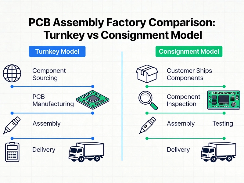
Turnkey PCB Assembly vs Consignment: Which Model Actually Fits Your Project?June/05/2026
What's the Difference Between Prototype PCB Assembly and Low Volume PCB Assembly ?May/18/2026
Accelerating Time-to-Market with Fast Prototype PCB AssemblyJune/10/2026
PCB Assembly FAQ: What Files Do I Need to Submit?June/17/2026