Open Nav



Yes, absolutely! Assembling printed circuit boards (PCBs) with components on both sides is not only possible but increasingly common in modern electronics manufacturing. This approach, known as double-sided or two-sided PCB assembly, allows engineers to maximize board space utilization, achieve higher component density, and create more compact electronic devices. From smartphones and wearable technology to industrial control systems and automotive electronics, double-sided assembly enables sophisticated functionality within limited form factors.
However, successful double-sided assembly requires careful planning, specialized equipment, and adherence to specific design and manufacturing guidelines. This comprehensive FAQ addresses the most common questions about assembling boards with components on both sides, helping you understand when to choose this approach, what challenges to expect, and how to ensure reliable, cost-effective production.
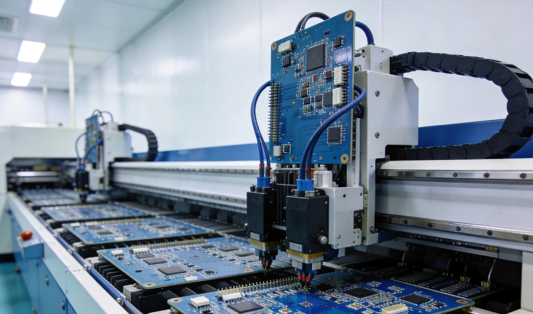
Double-sided PCB assembly refers to the process of mounting electronic components on both the top and bottom surfaces of a printed circuit board. Unlike single-sided assembly, where components reside exclusively on one side, double-sided boards utilize both surfaces to achieve higher component density and more complex circuit routing. This approach is particularly valuable when board real estate is limited or when designs require extensive functionality within tight space constraints.
The assembly process typically involves surface mount technology (SMT) components on both sides, though through-hole components may also be present on one or both sides depending on design requirements. Modern double-sided assembly primarily relies on SMT due to its compatibility with automated assembly equipment, smaller component footprints, and suitability for high-density layouts. The process requires specialized manufacturing equipment capable of handling boards during multiple reflow cycles without damaging components already mounted on the opposite side.
Double-sided PCB assembly follows a sequential process that builds up the board in stages, ensuring components on one side survive the thermal cycles required to solder components on the opposite side. The typical workflow includes:
The assembly process begins with the primary side, typically designated as the top side. Solder paste is applied to the board's top surface pads using stencil printing, followed by automated pick-and-place machines that position components precisely. The board then passes through a reflow oven where controlled heating melts the solder paste, creating permanent solder joints between components and the board. This first reflow cycle establishes reliable connections for primary side components without subjecting the yet-unassembled bottom side to thermal stress.
After primary side assembly completes and the board cools, the process repeats for the secondary (bottom) side. The board flips over, and solder paste is applied to bottom-side pads. Components are placed on the bottom surface, and the board undergoes a second reflow cycle. During this second reflow, previously soldered primary side components must remain securely attached despite being exposed to elevated temperatures again. This requirement drives specific process controls and component selection criteria for double-sided assembly.
For heavy components or designs where secondary side reflow temperatures approach the melting points of primary side solder joints, manufacturers may apply adhesive beneath primary side components before the first reflow. This adhesive provides mechanical reinforcement during the second thermal cycle, preventing components from shifting or detaching. The adhesive cures during the first reflow, creating a strong bond that supplements solder joint strength during subsequent processing.
Double-sided PCB assembly offers numerous benefits that make it attractive for many electronic product designs:
Utilizing both board surfaces effectively doubles the available mounting area for components. This increased density enables more functionality within the same board footprint or allows designers to reduce overall board size while maintaining or increasing capabilities. For space-constrained applications like wearable devices, mobile phones, and compact industrial controllers, double-sided assembly often represents the difference between feasible and impossible designs.
Components on both sides can facilitate more efficient signal routing. Designers can route traces between components on opposite sides more directly, potentially reducing layer count requirements and signal path lengths. Shorter trace lengths improve signal integrity, reduce electromagnetic interference, and enhance overall electrical performance, particularly important for high-speed digital circuits and sensitive analog applications.
While double-sided assembly adds manufacturing complexity, it can reduce overall system costs by enabling smaller board sizes, fewer layers, and potentially eliminating the need for additional boards or interconnects. For complex designs requiring extensive functionality, the cost savings from reduced board area and layer count may outweigh the added assembly expenses associated with double-sided processing.
Distributing power-generating components across both board surfaces can improve thermal management by spreading heat generation more evenly. This distribution can reduce localized hot spots, potentially improving reliability and simplifying thermal design requirements. Additionally, components on the bottom side may benefit from direct thermal contact with mounting surfaces or heat sinks in certain enclosure designs.
Despite its advantages, double-sided PCB assembly introduces specific challenges that designers and manufacturers must address:
Components on the primary side must withstand the reflow temperature profile for secondary side assembly. This exposure means primary side components experience two complete thermal cycles instead of one, potentially impacting reliability. Manufacturers must select components rated for multiple reflow cycles and carefully control reflow profiles to minimize thermal stress. Temperature-sensitive components may require special handling, adhesive reinforcement, or strategic placement on the secondary side to reduce thermal exposure.
Double-sided assembly essentially doubles the assembly steps compared to single-sided processing, increasing process complexity and potential failure points. Each additional reflow cycle introduces opportunities for defects like solder joint cracking, component misalignment, or tombstoning. Manufacturers typically implement stricter quality control measures for double-sided assemblies, including additional inspection steps and potentially lower acceptable defect rates, which can impact yield and cost.
Double-sided boards require careful DFM considerations to ensure manufacturability. Component placement must account for board handling during secondary side processing, avoiding areas where mechanical fixtures might contact components. Thermal relief patterns for ground connections need special attention to prevent heat from secondary side reflow from damaging primary side solder joints. Via-in-pad designs require additional consideration to prevent solder wicking away from component leads during secondary reflow.
Visual inspection of solder joints becomes more challenging with components on both sides, particularly when high-density layouts obscure visibility. Automated optical inspection (AOI) systems must inspect both surfaces, requiring longer inspection times and potentially more sophisticated equipment. Rework and repair operations also become more complex, as accessing components on one side may require temporary removal of components on the opposite side or specialized fixtures to protect already-soldered components during rework heating.
Successful double-sided assembly begins with proper design practices that address manufacturing requirements:
Choose components specifically rated for multiple reflow cycles, particularly for primary side placement. Check component datasheets for maximum reflow cycle specifications and thermal resistance characteristics. Place temperature-sensitive components, large electrolytic capacitors, and heavy components preferentially on the secondary side to minimize thermal stress. Maintain adequate spacing between components on opposite sides to prevent thermal interactions and ensure proper reflow soldering for both surfaces.
Design thermal relief patterns carefully for ground and power connections to balance heat transfer requirements with solder joint integrity during secondary reflow. Excessive thermal relief can prevent proper solder melting on the secondary side, while insufficient relief may cause primary side solder joints to reflow and potentially degrade. Consider using smaller pad sizes for secondary side components to reduce heat sinking and ensure proper solder joint formation during the second reflow cycle.
Strategically place vias to support assembly processes rather than interfere with them. Avoid placing vias directly under component bodies where they can create solder wicking issues during reflow. For double-sided designs, consider using filled and capped vias (via-in-pad) to create flat surfaces that improve solder paste printing and component placement accuracy. When using via-in-pad, ensure the via fill material and capping process can withstand both reflow cycles without degradation.
Board thickness affects thermal conductivity and mechanical stability during double-sided reflow. Thinner boards (0.8mm-1.0mm) may warp or flex more easily during thermal cycling, potentially causing component misalignment or solder joint issues. Standard 1.6mm thickness provides good mechanical stability, while thicker boards (2.0mm+) improve thermal mass but may require adjusted reflow profiles. Select PCB materials with appropriate thermal properties (glass transition temperature, coefficient of thermal expansion) that can withstand multiple reflow cycles without degradation.
Cost considerations for double-sided assembly involve multiple factors:
Double-sided assembly typically costs 20-40% more than single-sided processing due to additional manufacturing steps. The second stencil printing, component placement, and reflow cycle all add processing time and equipment utilization. Quality inspection costs also increase as both surfaces require verification. However, these increased assembly costs may be offset by savings from reduced board area, fewer layers, or simplified system architecture.
When double-sided assembly enables board size reduction or layer count decrease, material costs can decrease significantly. Smaller boards use less PCB material and copper, while fewer layers reduce dielectric material and processing complexity. For high-volume production, these material savings may substantially offset increased assembly costs, making double-sided assembly economically attractive overall.
Double-sided boards may require more extensive testing and validation, particularly for critical applications. Additional electrical testing, thermal cycling, and reliability validation increase non-recurring engineering (NRE) costs. However, these expenses typically occur once per design rather than per unit, so their impact diminishes with higher production volumes.
Yield rates for double-sided assembly may be slightly lower than single-sided due to increased process complexity and thermal stress. Lower yields increase effective per-unit costs by creating more scrap and rework. Working with experienced assembly providers and implementing robust DFM practices can minimize yield differentials, making double-sided assembly cost-competitive for many applications.
Double-sided assembly makes sense for specific design scenarios:
When product form factors limit board size but functionality requirements remain extensive, double-sided assembly often becomes necessary. Wearable devices, handheld instruments, compact medical equipment, and mobile electronics frequently rely on double-sided assembly to achieve required functionality within tight spatial constraints.
Complex digital designs with multiple processors, memory chips, interface circuits, and power management functions benefit from double-sided assembly. The ability to distribute logic, memory, and support circuits across both surfaces enables sophisticated functionality that would be impractical on single-sided boards of reasonable size.
For high-volume products where board area represents a significant cost driver, double-sided assembly can reduce overall system costs despite higher per-unit assembly expenses. The material savings from smaller boards and fewer layers often outweigh assembly cost increases at production volumes above 10,000-50,000 units.
Applications where heat generation must be distributed evenly benefit from double-sided component placement. Power electronics, LED drivers, and motor controllers often place power devices and thermal components on both sides to improve heat dissipation and reduce thermal stress on individual components.
Ensuring reliable double-sided assemblies requires comprehensive quality control:
AOI systems inspect both board surfaces after each reflow cycle, checking for component placement accuracy, solder joint quality, and common defects like tombstoning, bridging, or insufficient solder. Dual-sided AOI capability is essential for thorough verification, though inspection time increases proportionally with the number of surfaces to examine.
X-ray inspection becomes particularly valuable for double-sided assemblies, especially for ball grid array (BGA) components, quad flat no-lead (QFN) packages, and area array devices where solder joints are not visually accessible. X-ray technology verifies solder joint formation on both sides without requiring destructive testing or component removal.
Comprehensive electrical testing validates proper assembly and functionality for both sides simultaneously. In-circuit testing (ICT), flying probe testing, or functional testing verify connections, component values, and circuit operation. Test fixtures must access test points on both board surfaces, which may require specialized fixture design or dual-sided probe access.
Because double-sided assemblies experience multiple reflow cycles and potentially different thermal profiles during operation, reliability testing should include thermal cycling that simulates expected operating conditions. This testing helps identify potential solder joint fatigue issues or component degradation related to thermal stress from double-sided processing.
Yes, mixed technology double-sided assemblies combining through-hole and surface mount components are possible but add complexity. Through-hole components typically undergo wave soldering or selective soldering after SMT processes complete, meaning through-hole components on the secondary side may require special handling during secondary side reflow. Several approaches handle mixed technology:
The simplest approach places all through-hole components on the primary side, allowing standard double-sided SMT processing followed by a final wave or selective soldering operation for through-hole joints. This approach minimizes complexity while providing through-hole component benefits where needed for mechanical strength or high-current connections.
When through-hole components must reside on the secondary side, selective soldering equipment can solder these components after SMT processes complete without affecting already-soldered SMT components. Selective soldering applies molten solder only to specific through-hole joints using precise nozzles and shielding, protecting surrounding SMT components from thermal exposure.
For prototype or low-volume production, hand soldering of through-hole components after SMT assembly provides flexibility without requiring specialized selective soldering equipment. However, hand soldering introduces variability and potential quality issues that must be carefully controlled through operator training and process documentation.
Clear communication with your assembly provider ensures successful double-sided production:
Provide detailed assembly drawings that clearly indicate component placement on both surfaces, including side designations (top/bottom or primary/secondary). Document any special requirements like component adhesive application, reflow profile modifications, or inspection criteria specific to double-sided processing.
Clearly designate which components belong on each board surface in your bill of materials (BOM) and assembly documentation. Use consistent naming conventions (e.g., "Top Side" and "Bottom Side" or "Side A" and "Side B") to avoid confusion during assembly. Specify any components that require special handling due to thermal sensitivity or weight.
Document specific process requirements for double-sided assembly, including preferred reflow profiles, adhesive application specifications, and any special handling instructions. If you have preferences for which side should be assembled first (primary vs. secondary), specify this clearly as it affects process planning and thermal considerations.
Define quality standards and acceptance criteria for both surfaces, including acceptable defect levels, inspection requirements, and testing specifications. Reference relevant IPC standards (IPC-A-610 for acceptability, IPC-6012 for qualification) and specify any additional requirements specific to your application or industry.
Double-sided PCB assembly represents a powerful capability in modern electronics manufacturing, enabling higher component densities, more compact designs, and optimized functionality within limited board real estate. While the process introduces complexity and cost considerations compared to single-sided assembly, the benefits often outweigh the challenges for space-constrained applications, high-functionality designs, and cost-optimized high-volume production.
Success with double-sided assembly requires thoughtful design, careful component selection, clear communication with manufacturing partners, and robust quality control processes. By understanding the technical requirements, cost implications, and best practices outlined in this FAQ, you can make informed decisions about when and how to leverage double-sided assembly for your electronic products.
As electronics continue pushing toward smaller form factors and greater functionality, double-sided assembly will remain an essential tool in the designer's toolkit. Partner with experienced assembly providers who understand the unique challenges of double-sided processing, invest in proper DFM practices, and maintain clear documentation throughout the design-to-manufacturing workflow. With these approaches, double-sided PCB assembly delivers reliable, cost-effective solutions for even the most demanding electronic applications.
Yes, double-sided assembly is commonly used in high-reliability applications, but it requires additional design and process considerations. Components must be rated for multiple reflow cycles, thermal profiles must be carefully controlled, and more extensive reliability testing may be necessary. Working with assembly providers experienced in your industry's requirements ensures appropriate quality standards and processes are applied.
Double-sided assembly typically costs 20-40% more than single-sided processing due to additional manufacturing steps. However, overall project costs may be lower if double-sided assembly enables board size reduction, fewer PCB layers, or simplified system architecture. Calculate total landed costs including materials, assembly, and testing to determine the most economical approach for your specific design.
While boards up to 3.2mm thickness can undergo double-sided assembly, standard 1.6mm thickness provides good balance between mechanical stability and thermal characteristics. Thinner boards (0.8mm-1.0mm) may require special handling to prevent warping during thermal cycles, while thicker boards (2.0mm+) may need adjusted reflow profiles to ensure proper solder joint formation on both surfaces.
Yes, BGA components can be placed on both sides, but this introduces additional challenges. BGAs on the primary side must withstand secondary side reflow temperatures without solder joint reflow or degradation. X-ray inspection becomes particularly important for verifying BGA solder joint quality on both surfaces. Component selection and reflow profile control are critical for successful double-sided BGA assembly.
Several strategies prevent component detachment: using components rated for multiple reflow cycles, applying adhesive beneath heavy primary side components, controlling secondary side reflow temperatures to stay below primary side solder melting points, and designing adequate thermal relief for primary side connections. Working with your assembly provider to optimize reflow profiles and select appropriate components ensures reliable double-sided assembly.
Accelerating Time-to-Market with Fast Prototype PCB AssemblyJune/10/2026
What is Low Volume PCB Assembly?May/18/2026
What's the Difference Between Prototype PCB Assembly and Low Volume PCB Assembly ?May/18/2026
How Does Turnkey PCB Assembly Work? From BOM to Box BuildJune/29/2026
How to Evaluate a Reliable Prototype PCB Assembly PartnerJuly/29/2026