Open Nav



Populating both sides of a printed circuit board with surface-mount components is standard practice in modern electronics. It doubles component density without increasing board area, enables shorter signal paths, and often simplifies routing. But double-sided SMT assembly also introduces process complexity that single-sided builds never face—most critically, the challenge of running a board through reflow twice without disturbing components already soldered on the opposite side. Getting this right demands a disciplined process flow, careful material selection, and design decisions that anticipate manufacturing realities.
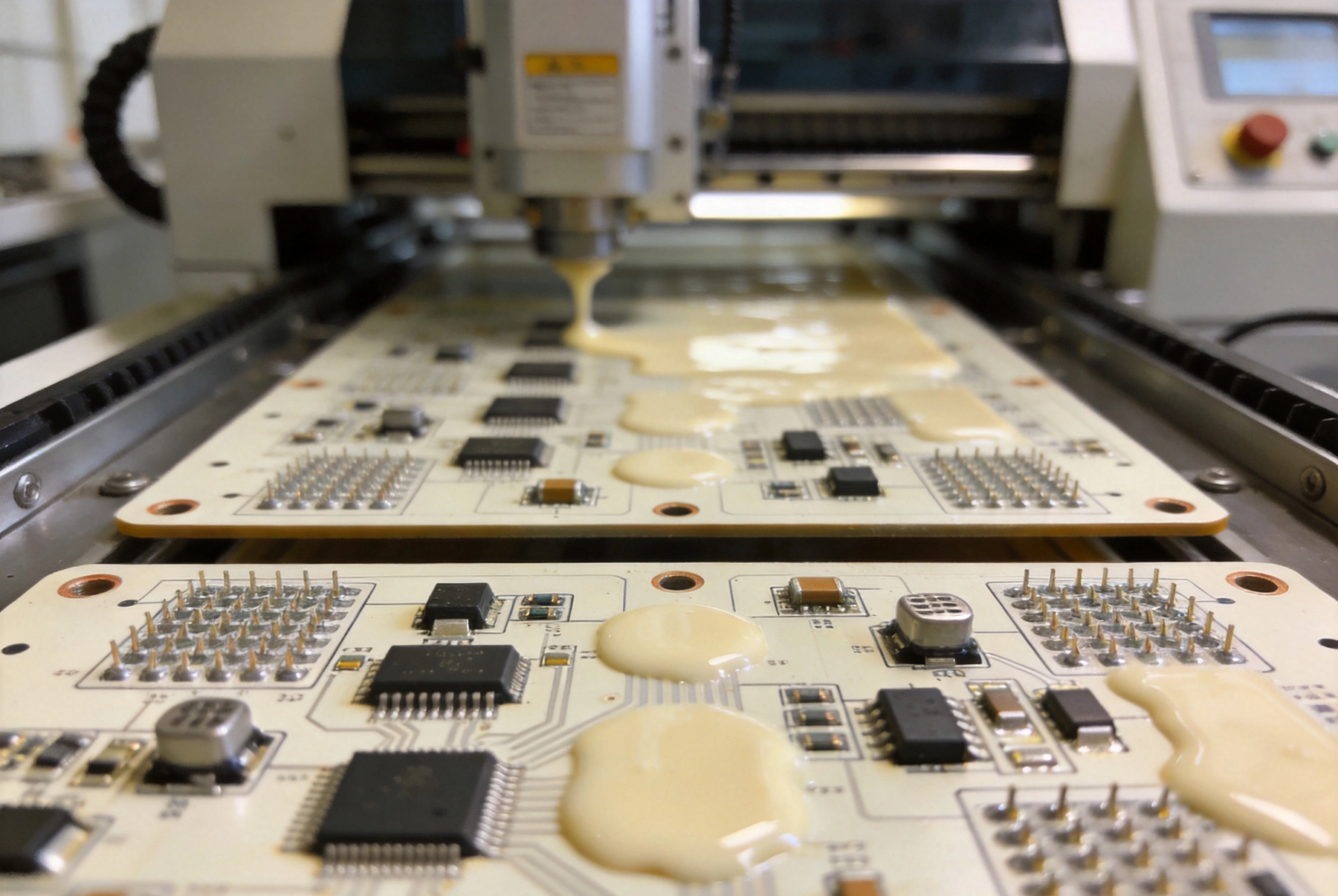
The fundamental sequence for double-sided SMT assembly follows a two-pass reflow model. Each pass solders one side of the board:
The critical question in step 7 is obvious: what prevents Side A components from dropping off when their solder joints re-melt during the second reflow pass? The answer depends on component mass, surface tension of the molten solder, and—when those forces are insufficient—the use of adhesive.
The convention is to reflow the side with larger, heavier components first (the primary side), and the side with smaller, lighter components second (the secondary side). The reasoning is straightforward:
In practice, the decision also depends on component distribution. If both sides carry BGAs or large connectors, adhesive staking on the primary side becomes mandatory. If one side is purely passives and small logic, it should be the secondary side.
When Side A reflows a second time, each component is held in place by two forces:
Molten solder has significant surface tension—approximately 0.47 N/m for SAC305 alloy at liquidus. For a typical 0603 resistor with two solder fillets, this force is roughly 0.15–0.25 N, which far exceeds the component's weight (about 0.004 N). Surface tension alone reliably holds small passives and most ICs during the second reflow.
Problems arise with heavier components. A 15 mm QFP, a large BGA, or a through-hole connector with substantial solder volume can generate a downward force that approaches or exceeds the available surface tension. The risk is not theoretical—components do tombstone, shift, or fall off during second reflow when this balance is unfavorable.
The rule of thumb: components with a mass-to-pad-area ratio exceeding approximately 0.5 mg/mm² are at risk during second reflow and require adhesive staking.
When surface tension alone cannot hold primary-side components during the second reflow, adhesive is applied before the first reflow to anchor them permanently.
The adhesive must cure before the second reflow. Two common approaches:
On the secondary side, solder paste must be printed with the board already populated on Side A. Warpage from the first reflow can affect stencil-to-board gasket integrity, causing paste smearing or insufficient deposition. Best practices:
Some assemblers use a lower-temperature solder paste on the secondary side (e.g., SAC305 with a reduced-peak profile) to minimize the time that primary-side joints spend above liquidus during the second reflow. This approach requires careful thermal profiling to ensure that secondary-side joints still achieve proper wetting and intermetallic formation while primary-side joints are not held above liquidus long enough to grow excessively thick intermetallic layers.
In most production environments, however, the same paste alloy is used on both sides and the thermal profile is simply optimized to minimize time above liquidus (TAL) during the second pass. Modern lead-free profiles typically achieve a TAL of 60–90 seconds, which is acceptable for SAC305 joints on both passes.
The second reflow profile must do two things simultaneously: fully reflow Side B solder joints, and re-heat Side A joints just enough to remelt them without causing damage. Key optimization targets:
Every second that a solder joint spends above liquidus grows the intermetallic layer. Excessive intermetallic growth embrittles joints and reduces thermal-cycle reliability. For the second pass, aim for the shortest TAL that still achieves full wetting on Side B—typically 60–75 seconds for SAC305.
Peak temperature on the second pass should be just high enough to ensure complete reflow across the board. For SAC305, a peak of 245–250 °C is typical. Avoid the temptation to run hotter "just to be safe"—every degree above the minimum accelerates intermetallic growth on Side A and increases the risk of component degradation, especially for moisture-sensitive devices.
A controlled ramp rate (1–2 °C/s) through the preheat zone prevents thermal shock to both components and the board. A soak zone at 150–180 °C activates flux on Side B and allows the board to reach thermal equilibrium before entering the reflow zone. This soak is especially important on the second pass because the board may have asymmetric thermal mass (Side A has more copper and components than Side B).
The easiest way to improve double-sided SMT yields is to make design decisions that simplify assembly. These DFM rules should be applied early—in the schematic and layout phase—rather than discovered during first-article builds.
Double-sided assemblies require inspection at multiple stages:
Symptom: After the second reflow, primary-side components are shifted, rotated, or missing.
Root causes: Insufficient surface tension (component too heavy), missing or inadequately cured adhesive, excessive peak temperature or TAL in the second profile, or vibration in the reflow oven conveyor.
Fix: Add adhesive staking for at-risk components, verify adhesive cure, and optimize the second-pass reflow profile to minimize TAL.
Symptom: X-ray reveals BGA solder balls partially immersed in the solder paste but not fully coalesced—forming a "head in pillow" shape.
Root causes: The second reflow can oxidize the existing primary-side solder surface, preventing proper wetting when the joint re-melts. Warpage of the BGA package or the board during the second thermal cycle can also physically separate the ball from the pad.
Fix: Use a nitrogen reflow atmosphere for the second pass to prevent oxidation, select BGAs with low-warpage substrates, and control board warpage through proper stack-up design.
Symptom: Secondary-side solder joints appear gray, grainy, or have reduced volume.
Root causes: Board warpage after first reflow causes poor stencil gasket, leading to reduced paste transfer. Stencil aperture blockage from paste left on the board-side of the stencil during Side B printing is also possible.
Fix: Use board-flattening fixtures during secondary-side printing, clean the stencil underside between prints, and verify paste volumes with SPI.
Symptom: Small passive components (0402, 0201) stand on one end after the second reflow.
Root causes: Uneven heating across the component due to asymmetric thermal mass on Side B, or unequal solder paste volume on the two pads (often caused by board warp degrading print quality).
Fix: Optimize reflow profile ramp rate for even heating, verify paste deposition symmetry with SPI, and reduce board warp with proper support during printing.
Many double-sided SMT boards also include through-hole components (connectors, headers, electrolytic capacitors). The standard approach is to place through-hole parts on the primary side and solder them using selective soldering or wave soldering after both SMT reflow passes are complete. This avoids exposing through-hole solder joints to two reflow cycles.
If through-hole components are placed on the secondary side, they must be soldered from below using selective soldering—which requires careful nozzle programming to avoid re-melting nearby secondary-side SMT joints. Pin-in-paste (intrusive reflow) is an alternative for through-hole parts with small lead counts, where solder paste is printed into the plated through-holes and the component is reflowed along with the surrounding SMT components. However, pin-in-paste on the secondary side adds paste volume to holes that may interfere with primary-side joints during the second reflow.
Double-sided SMT assembly is a well-established process, but it is not a simple extension of single-sided assembly. The second reflow pass demands careful consideration of component retention, adhesive strategy, thermal profile optimization, and inspection sequencing. By applying the best practices outlined here—segregating components by mass, staking heavy parts with adhesive, minimizing time above liquidus on the second pass, and inspecting after each reflow—you can achieve yields on double-sided builds that rival single-sided performance. The key is to design for the process from the start and to work with an assembly partner who understands the physics and process engineering behind every joint on both sides of the board.
Contact us to discuss your requirements.
Low Volume PCB Assembly: The Bridge Between Prototype and Mass ProductionJuly/07/2026
Advancements in Solder Paste Technology Transforming Electronics ManufacturingSeptember/03/2026
The Growing Demand for Low Volume, High-Mix Assembly ServicesSeptember/30/2026

Streamlining Production with Integrated PCB Fabrication and AssemblyJuly/20/2026
The True Cost of Poor Quality in PCB Assembly ServicesJuly/13/2026