Open Nav



In mass production, testing is not an afterthought—it is the gatekeeper that stands between a shipping dock full of defective boards and a customer who never complains. But testability does not happen by accident. It has to be designed in, from the earliest schematic entry through layout and all the way to panelization. Design for Testability (DFT) is the discipline of making your PCB easy, thorough, and affordable to test. This article covers the principles, strategies, and concrete implementation details that hardware teams use to build testability into every production board.
At prototype quantities, you can afford to probe each net by hand, run custom bench tests, and spend an hour debugging a single board. At 10,000 units per week, that approach collapses. You need automated tests that run in seconds, catch every significant defect, and produce actionable data for process improvement.
The cost of poor testability is not just in escapes—boards that pass test but fail in the field. It is also in test development time, fixture cost, low fault coverage, long debug cycles, and production bottlenecks. A well-designed DFT strategy pays for itself in the first production run; a poor one drains margin for the life of the product.
The fundamental trade-off in DFT is between test coverage and test cost. Every test point, every access via, every boundary-scan cell adds something to the board—area, complexity, component cost. The art of DFT is adding just enough test infrastructure to achieve the fault coverage you need, without bloating the design or the bill of materials.
DFT requirements differ depending on the test stage. Three principal test types dominate PCB mass production:
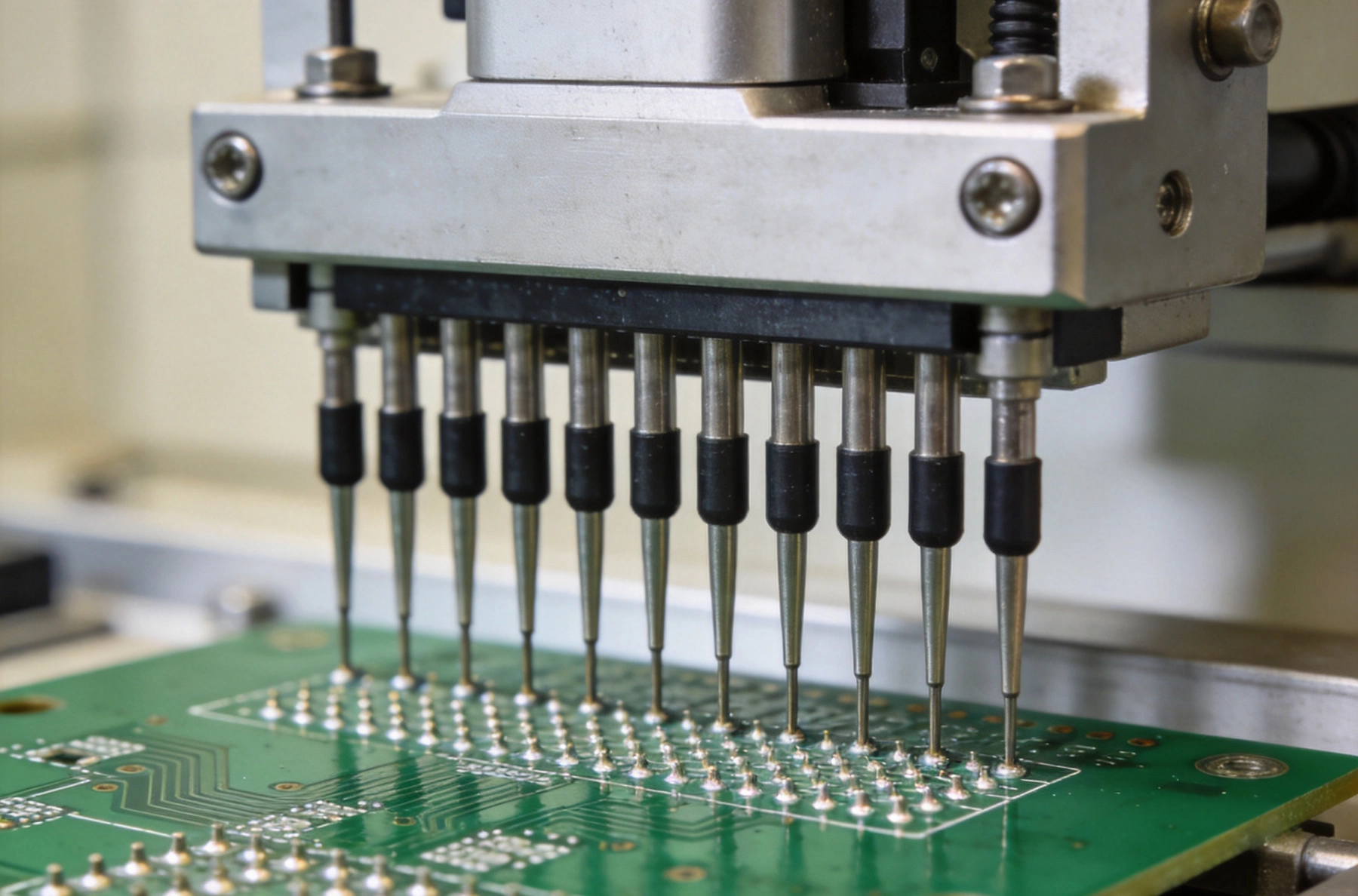
ICT uses a bed-of-nails fixture to simultaneously contact dozens or hundreds of nets, measuring component values, checking for opens and shorts, and verifying basic functionality. ICT is fast (a few seconds per board) and provides high fault coverage for manufacturing defects—but it requires physical access to nets, which means dedicated test points on the PCB.
The key DFT requirement for ICT is test point access. Every net that needs testing must have an exposed pad or via that a probe can reach from one side of the board (typically the bottom). Without access, ICT cannot test that net, and your fault coverage drops.
Flying-probe systems use moving heads to contact test points one at a time, checking opens, shorts, and some component values. No custom fixture is required, which eliminates tooling cost and lead time. The trade-off is speed—flying-probe takes minutes per board rather than seconds. It is best suited for low-to-mid volume production or as a bridge between prototype and full ICT deployment.
DFT for flying-probe is similar to ICT—test point access is essential—but the requirements are slightly relaxed because the probes can navigate around obstacles and access points on both sides of the board.
Functional test powers up the assembled board and verifies that it operates correctly—running firmware, checking outputs, measuring performance. FCT catches defects that ICT misses: wrong firmware, calibration errors, marginal timing, and system-level interactions. However, FCT is slower, more expensive to develop, and provides less diagnostic resolution than ICT.
DFT for functional test focuses on test connectors, debug headers, and software hooks that allow the test system to control and observe the board's behavior efficiently.
Test points are the physical interface between your board and the test system. Placing them correctly is the single most impactful DFT decision you will make.
Test points should be on one side of the board only—the side that the fixture probes from. This is almost always the bottom (solder) side. Placing test points on both sides requires a dual-side fixture, which doubles tooling cost and complexity.
Keep test points away from tall components—ICT probes need clearance to reach the board surface without interference. A common rule is 3–5 mm clearance between a test point and any component taller than 5 mm. Also maintain minimum spacing between test points themselves; 2.54 mm (100 mil) pitch is the traditional standard, though finer pitches are achievable with modern fixtures.
Arrange test points in a grid pattern where possible. Grid-aligned points simplify fixture wiring and reduce the chance of probe misalignment. Avoid placing test points near board edges, v-score lines, or breakaway tabs where board flexure during probing can cause contact reliability issues.
Use a consistent naming convention for test points in your schematic and layout. A common scheme is TP_<net_name> or TP<number>. Consistent naming makes it easier to generate test programs, debug failures, and correlate test results back to schematic nets.
An ICT fixture is a precision mechanical assembly. The board must fit it reliably, every time, with every probe making consistent contact. Several DFT practices ensure this:
Provide at least two, preferably three, tooling holes on the board for fixture registration. These should be on the board outline (not inside the keep-out area) and placed on a diagonal for maximum registration accuracy. Recommended diameter is 3.0 mm or 3.2 mm, unplated, with tight positional tolerance (±0.05 mm). The fixture uses hardened locating pins in these holes to position the board within the probe field.
Larger boards (above roughly 100 mm × 150 mm) need support under the board to prevent flexure when probes push down. Design support areas—clear zones with no components or traces—where the fixture can place support pins. Without adequate support, the board bends under probe pressure, causing intermittent contact and false test failures.
Every test point needs vertical clearance for the probe to reach the pad. Tall components near test points create shadows where probes cannot fit. Work with your test engineering team early in layout to identify clearance conflicts and move either the component or the test point.
Not every net can have a physical test point—especially on high-density designs with fine-pitch BGAs, dense routing, and limited board area. Boundary scan (IEEE 1149.1) provides test access through a serial interface rather than physical probes, making it invaluable for designs where ICT access is limited.
Boundary-scan-compliant components include a test access port (TAP) and boundary-scan cells on their I/O pins. By shifting test patterns through the JTAG chain, you can drive and observe pin values without physical access to the pins themselves. This enables testing of interconnections between boundary-scan devices—opens, shorts, and stuck-at faults on nets that connect two JTAG-compliant components.
The most effective test strategies combine boundary scan with ICT. Boundary scan covers the high-density nets around BGAs and fine-pitch devices where probes cannot reach. ICT covers the remaining nets, passive components, and power distribution. Together, they achieve fault coverage that neither can reach alone.
Functional test verifies system-level behavior—the board does what it is supposed to do when powered up and operating. DFT for functional test is about providing the test system with efficient control and observation paths.
Include dedicated test connectors that give the functional tester access to key signals: power rails, communication buses (UART, I2C, SPI), debug interfaces, and status outputs. These connectors should be on the board edge for easy cable or pogo-pin connection in the test station.
Work with firmware engineers to implement test-mode software that can be invoked by the test system. Common test hooks include:
These hooks should be accessible through a simple interface—often a single GPIO pin that puts the board into test mode at power-up, or a command over a serial debug port.
Large, complex boards benefit from test partitioning—dividing the design into independently testable subsections. This can be achieved with:
Power and ground nets are frequently overlooked in DFT planning because they seem "obvious." But power distribution defects—missing bypass capacitors, open power rails, ground plane voids—are among the most common manufacturing faults, and you need test access to catch them.
Place test points on every power rail, both at the source (regulator output) and at the load (IC power pins or nearby bypass capacitors). This allows ICT to verify that the rail is connected end-to-end and functional test to measure voltage under load.
Provide multiple ground test points distributed across the board. Ground is the reference for every measurement—bad ground contact causes false failures across the entire test. Multiple ground points give the fixture options and reduce the impact of any single contact failure.
DFT is not a layout-time activity. It starts at architecture and runs through every design phase.
Define test strategy: Which test types will be used (ICT, flying-probe, boundary scan, functional test)? What fault coverage target is required? What is the cost budget for test development and fixture tooling? These decisions constrain the DFT requirements that flow into schematic and layout.
Fault coverage is the percentage of potential manufacturing defects that your test can detect. It is the primary metric for DFT effectiveness and should be tracked explicitly.
Fault coverage = (detectable faults) / (total possible faults) × 100%. In practice, this is approximated by analyzing net access: if your test can access N out of M total nets, your raw access coverage is N/M. Real fault coverage depends on what you test on each accessible net—opens only, or opens plus shorts plus component values.
Target fault coverage depends on your product and industry. Consumer electronics may accept 95–97% coverage; automotive and medical devices typically require 99% or higher. The gap between your achieved coverage and 100% represents defects that will escape to the next test stage—or to the customer.
Many PCB design tools include DFT analysis features that automatically calculate test point coverage, identify untestable nets, and flag DFT rule violations. Run these checks as part of your design review, not as a post-layout afterthought. Coverage analysis early enough gives you time to add test points or boundary-scan devices to close the gaps.
The most common DFT mistake is treating test points as a layout cleanup task—sprinkling them in wherever space remains after component placement. This produces random test point distribution that complicates fixture design, reduces probe reliability, and often leaves critical nets untested. Test points should be placed intentionally, with the same care as component placement.
Reducing test points to save board area is a false economy. The board cost savings are minimal; the test cost increase—lower fault coverage, more escapes, longer debug—is significant. Define your minimum test point count during architecture and defend it during layout reviews.
Electronic design engineers often forget that the test fixture is a mechanical system. Test points too close to tall components, board edges, or other probes cause fixture reliability problems that show up as intermittent test failures on the production line. Collaborate with your test engineering team on layout reviews—they will catch issues that pure electrical review misses.
A test program that passes a known-good board is necessary but not sufficient. You also need to verify that the test catches known-bad boards. Create a set of defect-seeded boards (or use a fault-insertion test adapter) and confirm that your test detects each injected fault. This validation step—often called a "proof of test"—is essential for confidence in your test coverage claims.
Every DFT feature adds something to the board cost. Test points consume area. JTAG components may cost more than non-JTAG equivalents. Test connectors occupy board edge space. The key question: does the test cost savings justify the design cost increase?
As a general guideline:
Design for Testability is not optional for mass production—it is the bridge between design intent and manufacturing reality. A board that cannot be tested thoroughly and efficiently will either ship with latent defects or consume excessive time and money in test development and debug. The discipline of DFT—test point placement, fixture design considerations, boundary-scan architecture, functional test access, and coverage analysis—ensures that every production board gets the scrutiny it needs at a cost the business can sustain.
The best time to think about testability is at the beginning of the design, not the end. Build DFT requirements into your design checklist, run coverage analysis before layout freeze, and collaborate with test engineering throughout the development process. The result is a board that is not just well-designed, but well-tested—and that is what ensures quality in mass production.
Contact us to discuss your requirements for DFT-optimized PCB design and manufacturing.

Medical PCBA: Meeting Strict Regulatory Standards in AssemblySeptember/01/2026
Optimizing Component Spacing for Efficient PCB AssemblySeptember/10/2026

Top 10 DFM (Design for Manufacturability) Tips for SMT PCB AssemblyJune/08/2026

The Future of Flexible Hybrid Electronics (FHE) in AssemblyAugust/06/2026

Reducing Risk in Electronics Manufacturing with Full Turnkey ServicesAugust/15/2026