Open Nav



Every smartphone, smartwatch, and wireless earbud on the market contains a miracle of miniaturization—dozens of components crammed into spaces that would have seemed impossible a decade ago. The technology making this possible is high-density surface mount technology (SMT) assembly. While the concept sounds straightforward—place tiny components on a circuit board—the reality involves engineering challenges that push manufacturing capabilities to their limits.
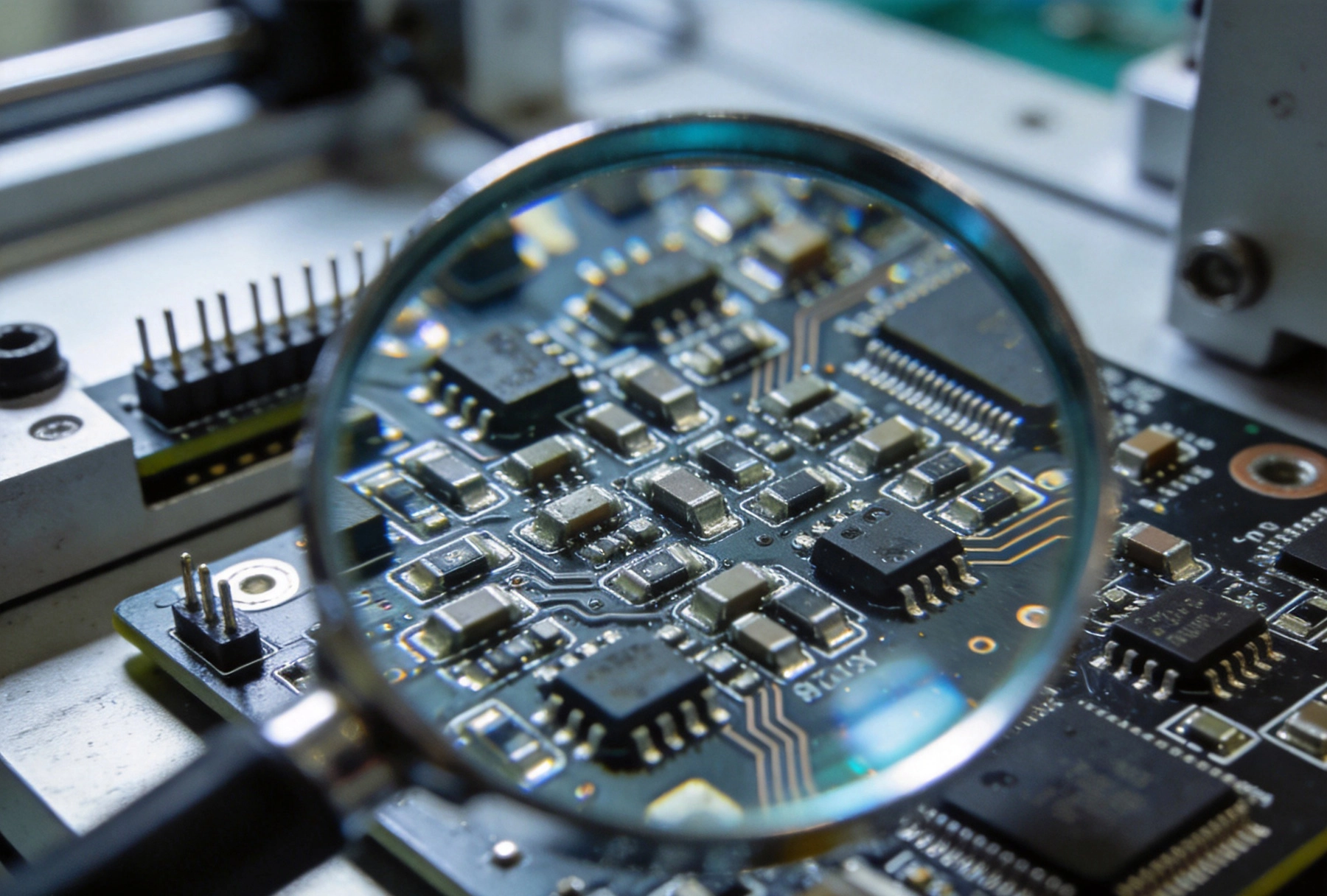
Consumer electronics manufacturers face constant pressure to pack more functionality into smaller form factors while maintaining quality and keeping costs manageable. This balancing act drives innovation in assembly techniques, equipment capabilities, and design methodologies. Understanding how high-density SMT assembly works helps product teams make better decisions during development.
The trajectory of consumer electronics has followed predictable paths: devices get smaller, more powerful, and more affordable over time. This evolution creates cascading requirements for assembly processes. What qualified as high-density ten years ago now barely registers as standard. Today's cutting-edge designs anticipate tomorrow's mainstream expectations.
High-density SMT assembly refers to mounting techniques that achieve component densities significantly above conventional levels. This manifests in several ways: reduced component packages (0201, 01005, and smaller), tighter spacing between components, more complex multi-layer boards, and advanced interconnection technologies like microvias and buried vias.
Market dynamics accelerate these changes. Product lifecycle compression means manufacturers must ramp production faster while maintaining first-pass yields. Competitive pricing pressure demands efficiency at scale. These constraints make high-density assembly capability a competitive necessity rather than a premium offering.
Passive components have followed aggressive miniaturization roadmaps. The familiar 0402 package (1.0mm x 0.5mm) has given way to 0201 (0.6mm x 0.3mm) in many applications, with 01005 (0.4mm x 0.2mm) appearing in space-constrained designs like smartphones and wearables.
Handling these tiny components requires precision placement equipment capable of sub-50-micron accuracy. Standard pick-and-place machines designed for larger components cannot maintain required yields at these scales. Manufacturers investing in high-density capability need equipment specifically engineered for micro-component handling.
The challenges extend beyond placement accuracy. Solder paste volume control becomes critical when pads measure fractions of millimeters. Insufficient paste creates weak joints; excess paste causes bridging between adjacent pads. Advanced stencil technology and precise paste printing processes address these issues, but they add complexity and cost to the assembly process.
Integrated circuits increasingly use area-array packaging rather than perimeter-lead formats. Ball Grid Arrays (BGAs), Quad Flat No-leads (QFNs), and land grid arrays (LGAs) offer electrical performance advantages and space savings, but they introduce assembly challenges that demand specialized expertise.
BGA components hide their interconnection points beneath the package. Solder joints form between the package bottom and board pads, invisible to visual inspection. Without X-ray inspection capability, manufacturers cannot verify joint quality. This represents a fundamental shift from inspection-based quality control to process-controlled quality assurance.
QFN packages present different challenges. Bottom-terminated leads require excellent coplanarity control and precise paste deposition. Void formation under thermal pads can cause reliability issues, particularly in applications with thermal cycling. Specialized underfill and thermal interface materials help, but they add processing steps and cost.
Package-on-Package (PoP) configurations stack memory packages atop processor packages, achieving vertical integration that saves board space. This approach is common in smartphones where board real estate comes at premium pricing. Assembly complexity increases substantially—misalignment during stacking can destroy expensive components.
Stacked die packaging integrates multiple chips into single packages, further reducing footprint. These configurations appear in microcontrollers, sensors, and specialized ICs where integration provides size and cost benefits. The assembly processes must accommodate warpage, coplanarity variations, and the inherent challenges of bonding bare die to substrates.
High-density interconnects (HDI) PCB technology enables the routing densities that modern consumer electronics require. Traditional through-hole vias consume substantial board area. HDI alternatives—microvias, blind vias, and buried vias—achieve similar connectivity while dramatically reducing space consumption.
Microvia technology allows connections between adjacent layers without consuming routing area on intermediate layers. A 0.15mm microvia occupies roughly 5% of the board area that a comparable through-hole via would consume. At consumer electronics volumes, these space savings translate directly to smaller, lighter products.
HDI manufacturing processes demand capabilities beyond standard multilayer board fabrication. Laser drilling creates microvia holes with diameters measured in fractions of millimeters. Sequential lamination builds up layer counts while maintaining alignment tolerances measured in microns. These processes require specialized equipment and highly trained personnel—standard PCB manufacturers may lack the capability or experience for HDI work.
Solder paste printing determines assembly quality more than any other single process. For high-density designs, paste deposit variations that would be acceptable for standard components become catastrophic. Achieving consistent paste volumes requires printer precision, stencil quality, and board support systems that minimize deflection during printing.
Stencil technology has evolved to meet high-density requirements. Laser-cut stencils with electroformed walls achieve sharper paste release than conventional chemical etch stencils. Nanocoatings reduce paste adhesion to stencil walls, improving transfer efficiency. These improvements matter when depositing paste on 0.3mm pads—marginal performance becomes unacceptable.
Inspection of paste deposits before component placement catches many defects before they become costly problems. Solder Paste Inspection (SPI) systems measure deposited volume and shape, flagging boards that deviate from specifications. Integrating SPI into production lines adds cost but improves first-pass yields by enabling real-time process adjustments.
Modern placement equipment achieves placement accuracies of 30-50 microns for standard components, with specialized systems reaching sub-20-micron performance for micro-components. This precision requires closed-loop feedback systems that measure actual placement positions and correct deviations in real-time.
Vision systems have become increasingly sophisticated to meet high-density requirements. Multiple camera stations inspect components before, during, and after placement. Advanced algorithms compensate for component variation, board warpage, and conveyor positioning errors. The goal is consistent placement regardless of the inevitable variations in real-world manufacturing conditions.
feeder technology also impacts high-density assembly. Vibration feeders for tape-and-reel components must deliver parts with consistent orientation and spacing. Vision-guided part presentation identifies part rotation and corrects it automatically. For components with ground planes or reflective surfaces, specialized lighting techniques improve recognition accuracy.
Reflow soldering must achieve complete wetting across diverse component types simultaneously. Large BGAs, tiny 01005 passives, and thermal mass variations across board areas create conflicting thermal requirements. A reflow profile optimized for one condition may be suboptimal—or damaging—for another.
High-density boards often require careful thermal profile development. Thermocouple attachment to critical components enables precise profiling that accounts for actual board thermal characteristics. Multiple thermal zones in reflow ovens allow finer control over heating rates and soak periods. For lead-free alloys, profile optimization becomes even more critical due to narrower process windows.
Automated Optical Inspection (AOI) works well for components with visible terminations. For bottom-terminated components like QFNs and BGAs, AOI cannot see the critical joints beneath packages. Relying solely on AOI creates inspection gaps that can allow defective boards to proceed through production.
X-ray inspection becomes essential for high-density assemblies. Two-dimensional X-ray reveals voiding, bridging, and other defects hidden from optical inspection. Computed Tomography (CT) scanning provides three-dimensional reconstruction of hidden joints, enabling detailed analysis of complex structures. While CT is too slow for production inspection, it serves valuable roles in failure analysis and process development.
High-density boards often have reduced test access due to component placement obscuring test points. Flying probe testers can access more points than traditional bed-of-nails fixtures, but they operate slower and may still struggle with densely packed designs.
Design for Testability (DFT) practices become valuable for high-density products. Including test points, providing probe access, and designing clearances for fixture pins all improve test coverage. Boundary scan architecture (IEEE 1149.x) can verify connections for JTAG-compatible devices even when physical access is limited.
Understanding typical defects helps quality teams focus inspection resources effectively. High-density assembly defects often stem from the same root causes: paste issues, placement accuracy, reflow problems, or design limitations.
Tombstoning—where small components stand up on one end during reflow—occurs more frequently with miniaturized components. Thermal imbalance between component terminations causes asymmetric wetting forces. Paste volume consistency and component placement accuracy both affect tombstone frequency.
Head-in-pillow defects occur when BGA solder balls and paste deposits form incomplete融合 during reflow. The joint looks connected but lacks reliable metallurgical bonding. This defect is difficult to detect with standard inspection and can cause field failures. Proper reflow profiling and clean board surfaces help prevent this issue.
bridging between adjacent pads occurs when excess solder or poor paste release creates unintended connections. High-density designs with closely spaced pads are particularly susceptible. Stencil quality and paste printing control directly impact bridging frequency.
High-density assembly requires components that meet stringent tolerances. Not all component manufacturers produce parts suitable for high-density applications. Verify that suppliers can consistently deliver components meeting required specifications—variations that would be acceptable for standard products may cause assembly problems in dense designs.
Component packaging affects manufacturing efficiency. Waffle packs and matrix trays accommodate high-density component handling better than standard tape-and-reel for some part types. Work with suppliers to specify appropriate packaging for your assembly process.
Long-term component availability deserves attention even for fast-moving consumer products. Product lifecycles may extend longer than anticipated, particularly for successful products. Identify alternative components early in development to avoid costly redesigns if primary sources become unavailable.
Not all contract manufacturers have the capability or experience for high-density assembly. Evaluate potential partners on multiple dimensions: equipment capabilities, process experience, quality systems, and track record with similar products.
Equipment age and maintenance affect capability. Modern placement systems offer capabilities that older equipment cannot match. Ask about equipment specifications, maintenance schedules, and calibration procedures. Capabilities that sound adequate may fall short when you examine details.
Experience with similar products matters more than general capability claims. A manufacturer with extensive experience assembling smartphones will have different strengths than one focused on automotive electronics. Look for relevant case studies and ask about specific challenges they've encountered with similar designs.
Commercially, 01005 (0.4mm x 0.2mm) is currently the practical minimum for volume production. Smaller packages exist in research contexts but face manufacturing challenges that limit commercial viability. Most high-density consumer products use a mix of 0402, 0201, and 01005 depending on space constraints and cost considerations.
High-density assembly typically costs 30-100% more than standard SMT assembly due to equipment requirements, process complexity, and lower first-pass yields during learning curves. Exact premiums depend on board complexity, volumes, and manufacturer capabilities. The cost premium often makes sense given the functionality and size benefits high-density designs provide.
Main reliability concerns include thermal cycling tolerance (particularly for mixed component sizes), mechanical shock resistance (especially for droppable devices), and long-term solder joint integrity. Design for Manufacturability (DFM) reviews help identify potential reliability issues before production begins. Accelerated life testing validates reliability assumptions.
Many existing lines can accommodate moderate high-density requirements with process adjustments. However, extreme miniaturization typically requires dedicated equipment optimized for micro-component handling. Manufacturers considering high-density products should evaluate whether existing equipment can achieve required yields or whether investment in specialized capability is necessary.
Provide complete manufacturing data packages including Gerber files, drill files, component placement data, and Bill of Materials. For high-density designs, include IPC-7351 land pattern specifications and any special handling requirements. Clear communication with your assembly partner about design intent helps avoid surprises during production.
High-density SMT assembly represents a convergence of design ambition and manufacturing capability. Consumer electronics continue pushing toward smaller, more capable products, and assembly processes evolve to meet these demands. Success requires attention to design practices, component selection, manufacturing capabilities, and quality control throughout development.
Product teams that understand high-density assembly challenges can make better tradeoffs during design. Sometimes accepting slightly larger packages or adding test points improves manufacturability without compromising product goals. Early engagement with capable manufacturing partners helps identify potential issues before they become expensive problems.
The consumer electronics market rewards efficiency and innovation. High-density assembly capability enables products that would be impossible otherwise—smaller sizes, more features, better performance. Manufacturers that master high-density SMT assembly gain competitive advantages that translate directly to market success.
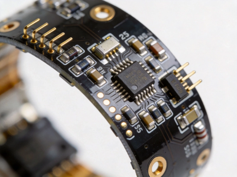
Precision SMT PCB Assembly for Wearable TechnologyJune/16/2026

Inventory Management Benefits of Using a Turnkey Assembly PartnerAugust/03/2026
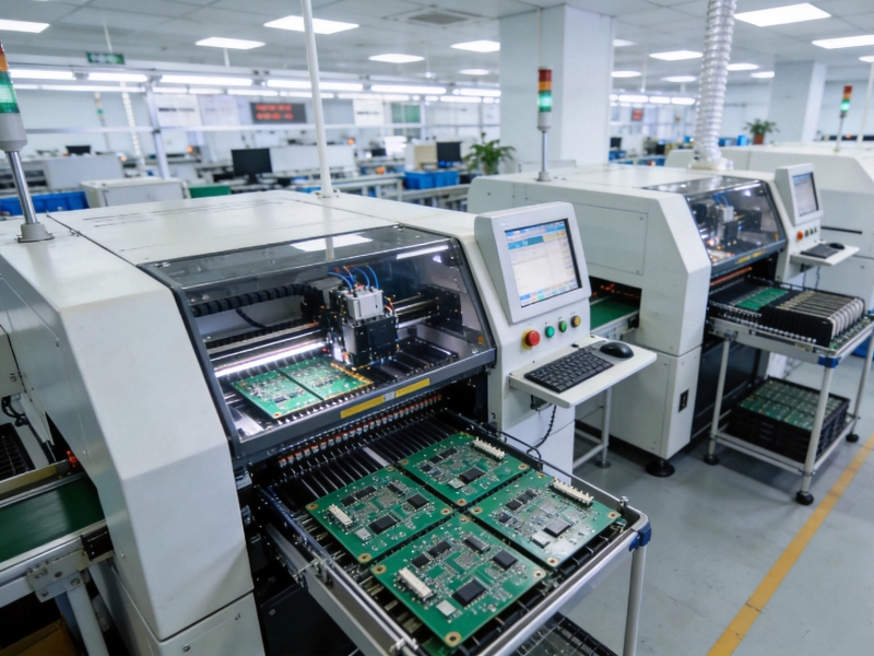
Reducing Risk in Electronics Manufacturing with Full Turnkey ServicesAugust/15/2026

The Rise of AI in SMT Quality InspectionJune/18/2026
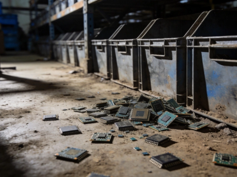
How the Global Chip Shortage is Impacting PCB Assembly ServicesJuly/23/2026