Open Nav



There is nothing quite like the frustration of opening the box from your assembly house, powering up your prototype, and finding that it does not work. Whether the board is completely dead, exhibits intermittent behavior, or fails only under specific conditions, a failed prototype assembly can derail your development timeline and consume debugging hours that should have been spent on feature development.
The good news is that most Prototype PCB Assembly failures follow predictable patterns. Understanding these patterns—and knowing how to systematically diagnose them—can dramatically reduce your time-to-root-cause and help you avoid making the same mistakes on your next build.
This guide walks through the most common reasons prototype assemblies fail, organized by where in the process the problem originates: the design, the fabrication, the assembly process, or the components themselves.
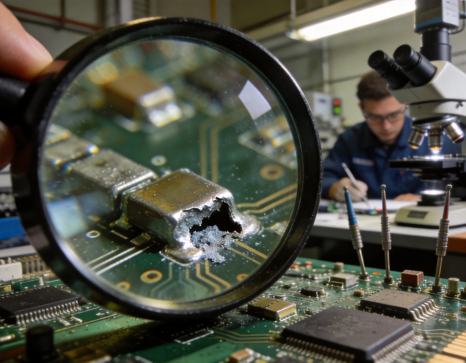
Many prototype failures are baked in before the board ever reaches the assembly line. Design errors are particularly insidious because they affect every single unit in the build—you cannot troubleshoot your way out of a fundamental design mistake.
This is arguably the single most common cause of prototype failure. If the land pattern for a component does not match the component's actual package—wrong pad sizes, incorrect pad spacing, or missing thermal pads—the solder joints will be unreliable at best and completely non-functional at worst.
The problem is especially prevalent with components sourced from multiple vendors that share the same part number but have subtly different package variants. A BGA with a 0.8mm pitch from one vendor may have slightly different ball diameters or body dimensions than the "same" BGA from another vendor. Always verify land patterns against the specific component's datasheet, not a generic library symbol.
How to diagnose: Inspect solder joints under magnification. If pads appear too large or too small relative to the component terminals, or if components are visibly misaligned after reflow, the footprint is likely wrong.
Vias and pads connected to large copper planes without proper thermal relief spokes can cause two problems: during soldering, the plane acts as a heat sink that prevents the pad from reaching reflow temperature, resulting in cold or incomplete solder joints; after assembly, the lack of thermal relief can make rework nearly impossible because you cannot deliver enough heat to the joint to melt the solder.
How to diagnose: Use a thermal camera during power-up. Pads with poor thermal connections will show temperature anomalies. Alternatively, measure resistance between the pad and the plane—it should be near zero, not tens of milliohms.
For prototypes, debug access is critical. If you did not include test points for key signals—power rails, critical control signals, communication bus lines—you will find yourself trying to probe tiny component pads with oscillating signals, which is a recipe for frustration and accidental shorts.
How to diagnose: If you are struggling to probe signals during debug, this is the root cause. Fix it in the next revision by adding dedicated test point pads with sufficient clearance for probe tips.
Prototype builds often reveal signal integrity issues that simulation did not catch—particularly when the actual PCB stackup differs slightly from the modeled one. Impedance mismatches cause reflections, crosstalk between parallel traces corrupts data, and insufficient decoupling creates power distribution network (PDN) noise that destabilizes voltage-sensitive circuits.
How to diagnose: Use an oscilloscope with appropriate bandwidth to check signal edges for ringing, overshoot, and undershoot. Check eye diagrams on high-speed serial links. Measure power rail ripple and transient response under load steps.
Even with a perfect design, defects introduced during board fabrication can cause assembly failures. Prototype runs—especially quick-turn orders—are more susceptible to fabrication defects because there is less process optimization and fewer inspections than in production runs.
If the drilled holes are misaligned relative to the copper layers, vias may have reduced annular rings or even break out entirely, creating open circuits. This problem is more common on boards with many layers where the accumulation of registration errors across multiple lamination cycles pushes drills off-center.
How to diagnose: Check via continuity with a multimeter—vias with broken annular rings will show open circuits. Cross-section a suspect via if you have the capability; the off-center drill will be immediately visible.
Voiding in the copper plating of through-holes and vias is a common fabrication defect, particularly in boards with high aspect ratios (thick boards with small holes). These voids can create high-resistance connections or open circuits, and they tend to worsen over time as thermal cycling stresses the plating.
How to diagnose: Electrical testing should catch completely open vias. Partial voids may pass electrical test but fail under thermal stress. If certain circuits work at room temperature but fail after the board warms up, plating voids are a prime suspect.
Under-etching leaves residual copper between closely spaced traces, creating short circuits that may be invisible to the naked eye. Over-etching narrows traces below their designed width, increasing resistance and potentially causing trace blow-outs under high current. Both problems are more likely on prototype runs where the etch process has not been finely tuned for the specific board design.
How to diagnose: Short circuits between adjacent nets will show up in electrical testing or cause excessive current draw at specific power rails. Visual inspection under magnification can sometimes reveal copper residues between fine-pitch traces.
If the board layers separate—either fully (delamination) or partially (measling/crazing)—the electrical connections between layers can be disrupted. This is often caused by moisture absorption in the laminate before lamination, inadequate lamination pressure or temperature, or a mismatch in the coefficients of thermal expansion between different laminate materials in a hybrid stackup.
How to diagnose: Visual inspection reveals white crosses or spots (measling) on the board surface. Delamination may be visible at board edges. Thermal cycling will worsen the problem—if failures increase with cycling, delamination is likely involved.
The assembly process—solder paste application, component placement, and reflow—is where the most visible and easily diagnosed failures occur. These are also the defects most likely to be caught by post-assembly inspection, but only if the inspection is actually performed.
The solder paste printing step is responsible for a majority of assembly defects. Common problems include:
How to diagnose: Solder paste inspection (SPI) equipment can catch these defects before components are even placed. Without SPI, inspect the board after reflow—insufficient paste shows as dull, concave joints; excess paste shows as bridging or bulging joints.
Pick-and-place machines are remarkably accurate, but on prototype runs—especially with short setup times and potentially unfamiliar components—placement errors do happen. Common issues include:
How to diagnose: Automated optical inspection (AOI) catches most placement errors. Manual inspection under magnification works for larger components, but fine-pitch parts may require X-ray to verify placement accuracy.
The reflow oven's thermal profile must deliver the right temperature at the right time to every joint on the board. Problems include:
How to diagnose: Attach thermocouples to the board and run it through the oven with a data logger to verify the actual profile matches the target. Inspect joints for signs of under-reflow (grainy, dull appearance) or over-reflow (excessively shiny, charred flux residues).
Small chip components—especially 0201 and 01005 sizes—can stand on one end during reflow if the solder on one pad melts before the other. The surface tension of the liquid solder pulls the component upright like a tombstone. This is caused by unequal thermal mass on the two pads (one connected to a large copper plane, the other isolated), asymmetric solder paste volumes, or uneven heating across the component.
How to diagnose: Visual inspection is sufficient—tombstoned components are immediately visible. Fix the root cause by balancing thermal relief on both pads, ensuring equal paste volume, and verifying the reflow profile provides uniform heating.
D3>Head-in-Pillow DefectsIn BGA packages, a solder ball can partially collapse onto its pad without forming a true metallurgical bond. The joint looks acceptable from the outside but has a gap at the interface that creates an open or high-resistance connection. This defect is caused by component warpage during reflow—package corners lift away from the board, separating balls from pads—and is aggravated by moisture in the BGA substrate.
How to diagnose: X-ray inspection is required; head-in-pillow defects are invisible from the outside. The X-ray image shows the ball sitting on the pad with a visible gap or non-contact area. Baking the BGA per its moisture sensitivity level (MSL) before assembly can prevent this defect.
Sometimes the board and the assembly process are both fine, but the components themselves are the problem.
Many surface-mount components—particularly BGAs, QFNs, and other plastic-encapsulated packages—absorb moisture from the atmosphere. When these components are rapidly heated during reflow, the absorbed moisture expands as steam and can cause "popcorning"—internal delamination or cracking of the package. This damage may not cause immediate electrical failure but creates a latent defect that shortens the component's life.
How to diagnose: If components fail after thermal cycling or after a period of field operation, popcorning damage is a likely cause. Prevention is the best approach: follow the component's MSL rating, store components in moisture-barrier bags, and bake exposed components before assembly per IPC/JEDEC J-STD-033.
Prototype builds, with their urgent timelines and sometimes informal sourcing, are vulnerable to counterfeit components—especially for parts in short supply or obsolete. A counterfeit IC may be a remarked different part, a reclaimed component from recycled boards, or a production reject sold on the gray market. These parts may sort-of work—passing basic functional tests but failing under stress, at temperature extremes, or at speed.
How to diagnose: If a component passes simple tests but fails under corner conditions (voltage extremes, temperature extremes, maximum speed), suspect a counterfeit or out-of-spec part. Verify component markings, check date codes for consistency, and source critical components from authorized distributors only.
Even legitimate components from authorized sources occasionally arrive non-functional—damaged by ESD during handling, killed by out-of-spec electrical stresses during prior testing, or simply defective from the factory. On a prototype with minimal test coverage, one dead component can make the entire board appear to fail in mysterious ways.
How to diagnose: Isolate suspect components by testing them out of circuit where possible. Check power consumption at each rail—a dead IC often draws no current or excessive current compared to its specification.
When your prototype does not work, resist the urge to start changing things randomly. A systematic approach will get you to the root cause faster and with more confidence.
Before applying power, examine the board carefully under magnification. Look for solder bridges, missing components, tombstones, cold joints (dull, rough appearance), and damaged components. Many problems are visible if you take the time to look.
Apply power and immediately check all voltage rails before anything else. If the power rails are wrong, nothing else will work correctly. Check for rails that are at the wrong voltage, rails with excessive noise or ripple, and rails that are pulling excessive current (indicating a short circuit or damaged component).
If power is good, verify that all clock signals are present and at the correct frequencies. Check that reset signals are properly asserted and released. A processor with no clock or a stuck reset will appear completely dead even though the hardware may be fine.
Trace critical signals from source to destination. Start with communication buses (SPI, I2C, UART)—verify that signals are present, at correct logic levels, and timing properly. A single stuck bus line can prevent an entire subsystem from functioning.
If you have identified a suspect area, isolate components within that area. Lift pins if necessary to test individual components out of circuit. Replace suspect components with known-good parts and observe whether the problem resolves.
If you have a working board—perhaps a previous revision or a development kit—compare signals between the working and failing boards. Differences in signal levels, timing, or noise can pinpoint the problem area quickly.
Troubleshooting is valuable, but prevention is better. Here are practical steps to reduce the chances that your next prototype assembly fails:
Prototype PCB Assembly failures are frustrating but rarely mysterious. The vast majority fall into the categories described in this guide: design errors like incorrect footprints, fabrication defects like drill registration and plating voids, assembly process failures like solder paste and reflow problems, and component issues like moisture damage and counterfeit parts.
The key to efficient troubleshooting is a systematic approach: visual inspection first, then power rail verification, then clock and reset checks, then signal tracing, and finally component isolation. Random probing and component swapping will eventually find the problem, but it wastes time and can introduce new problems.
Even more important than troubleshooting is prevention. Investing time in DFM review before tape-out, specifying appropriate inspection steps during assembly, and sourcing components carefully pays enormous dividends in first-pass prototype success rates. A prototype that works the first time does not just save money—it accelerates your entire development program.
Need a prototype assembly partner who gets it right the first time? Contact our team to discuss your prototype requirements, our inspection capabilities, and how we can help you avoid the common failure modes that derail development timelines.

Wave Soldering vs. Selective Soldering for Through-Hole Components: Which Process Wins?July/15/2026

Accelerating Time-to-Market with Fast Prototype PCB AssemblyJune/10/2026

What is the Difference between Class 2 and Class 3 PCBA?September/02/2026
FAQ: Can You Assemble Boards with Components on Both Sides?July/22/2026
How Long Does Prototype PCB Assembly Usually Take?July/09/2026