Open Nav



The solder alloy question is one of the most consequential decisions in electronics assembly, and one of the most misunderstood. For decades, tin-lead solder was the unquestioned standard, a reliable workhorse that most engineers never questioned because there was no reason to. Then environmental regulations like RoHS changed everything. Lead was restricted, the industry scrambled to find alternatives, and suddenly every assembly engineer had to understand the trade-offs between the old and the new. More than fifteen years after RoHS took effect, the debate has matured but not resolved. Leaded solder still exists in non-consumer applications, lead-free has become the default for most commercial products, and the technical trade-offs between them remain real and relevant. Understanding what each option actually offers helps engineers make informed decisions rather than defaulting to whichever alloy their competitors use.
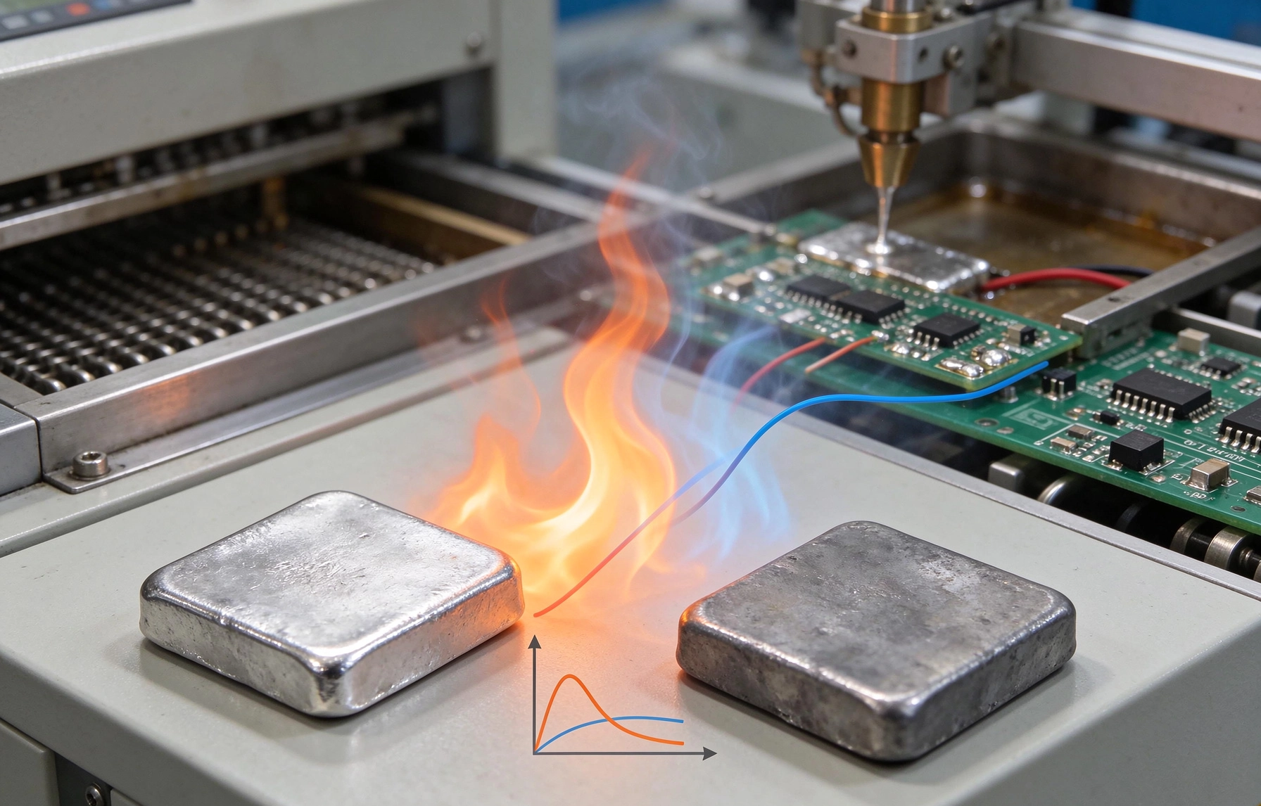
The choice of solder alloy affects nearly every aspect of PCB assembly, from the design rules that govern pad geometry to the reflow profile that determines how components are attached to the process controls that ensure consistent quality. Solder is not just a mechanical connection. It is an electrical connection, a thermal path, and a structural element that must withstand thermal cycling, vibration, mechanical shock, and long-term creep. The alloy determines how well the joint performs all of these functions across the product lifecycle.
The mechanical properties of the joint, including its strength, ductility, and resistance to fatigue, differ significantly between leaded and lead-free alloys. These differences manifest in reliability outcomes that vary with application environment, thermal cycling range, and product lifecycle expectations. A joint that performs excellently in one application may fail prematurely in another simply because the alloy was not matched to the requirements. Understanding these interactions is what separates engineers who get reliable assemblies from those who debug field failures.
The process requirements for each alloy also differ in ways that affect manufacturing cost, equipment requirements, and defect rates. Lead-free alloys generally require higher peak reflow temperatures, different flux chemistries, and tighter process control than traditional tin-lead alloys. These requirements have real cost implications that affect the economics of assembly choices. Pretending otherwise leads to surprises when the actual process costs emerge.
Tin-lead solder, typically with a composition of 63% tin and 37% lead by weight for the eutectic alloy, offers a combination of properties that has made it the standard for electronics assembly for over fifty years. The eutectic composition melts at 183 degrees Celsius, which is low enough to be compatible with most electronic components and substrate materials while being high enough to maintain joint integrity during normal service. The addition of lead to tin reduces the surface tension of the solder, which improves wetting behavior and produces smoother, more reliable fillets.
The mechanical properties of tin-lead solder joints are particularly favorable for thermal cycling reliability. The lead component adds ductility to the joint, allowing it to accommodate the stress from thermal expansion mismatch between components and substrates without cracking. Tin-lead joints tested in thermal cycling show better fatigue resistance than lead-free joints in many configurations, particularly for components with high thermal mass like BGAs and large capacitors. This reliability advantage is why leaded solder remains preferred for high-reliability applications where the cost of failure is high.
Wetting behavior is another area where leaded solder excels. The lower surface tension of tin-lead solder means it flows more readily onto properly prepared surfaces, producing better fillet formation and more consistent joint quality across a board. This wetting advantage becomes more significant as feature sizes decrease and pad geometries become more demanding. Fine-pitch components with 0.5mm pitch or smaller are easier to assemble reliably with leaded solder because the improved wetting reduces the risk of bridging while ensuring complete fillet formation.
The lower reflow temperature of leaded solder, 183 degrees Celsius for eutectic tin-lead versus 217 to 245 degrees for common lead-free alloys, reduces the thermal stress on components and substrates during assembly. This lower temperature window provides more margin against damage from peak temperature overshoot and accommodates components with lower temperature ratings. For assemblies that include temperature-sensitive components or substrates with lower glass transition temperatures, the leaded solder temperature window may be essential.
The environmental case for lead-free solder is straightforward: lead is a toxic heavy metal that accumulates in the environment and in biological systems, and reducing lead exposure from electronic products is a legitimate public health goal. RoHS and similar regulations reflect the consensus that the environmental burden of lead in electronics outweighs the technical benefits of tin-lead solder. Even setting aside regulatory compliance, many companies choose lead-free assembly to reduce the environmental footprint of their products and to align with corporate sustainability commitments.
Lead-free solder alloys have improved substantially since the initial rush to replace tin-lead in the early 2000s. Early lead-free alloys were problematic, with issues including poor wetting, high reflow temperatures, tin whisker formation, and reduced thermal cycling reliability. Modern lead-free alloys, particularly those based on tin-silver-copper, SAC, compositions, address many of these early concerns and provide reliable performance in a wide range of applications. The lead-free alloys of today are not the same as the lead-free alloys of fifteen years ago.
The higher reflow temperature required for lead-free solder can actually be an advantage in some applications. Higher temperature exposure during assembly serves as a screening mechanism that identifies weak components or substrates before they reach the field. Components that cannot survive the lead-free reflow profile would have failed early anyway in demanding applications. This high-temperature screening reduces the risk of field failures from components that are marginal at lower temperatures.
Lead-free solder joints tend to be harder and stronger at room temperature than tin-lead joints, which can be advantageous for applications subject to mechanical shock or vibration. The higher strength of lead-free joints resists deformation under mechanical load, which can improve reliability in automotive, aerospace, and industrial applications where vibration is a concern. This strength advantage must be balanced against the reduced ductility that makes lead-free joints more susceptible to fatigue under thermal cycling.
The reliability comparison between leaded and lead-free solder is not universal. It depends heavily on the application environment, the thermal cycling range, the product lifecycle expectations, and the specific alloys being compared. Drawing general conclusions without specifying the context leads to confusion and misapplication of the data.
For thermal cycling environments with moderate temperature ranges, typical of indoor electronics or consumer products, lead-free SAC alloys show reliability that is comparable to tin-lead in most configurations. The initial concerns about lead-free thermal cycling reliability have been largely addressed through improved alloy compositions and better understanding of the failure mechanisms. Modern lead-free assemblies meet the reliability requirements of the vast majority of commercial applications.
For extreme thermal cycling environments with large temperature ranges, particularly those with temperatures below freezing or above 100 degrees Celsius, leaded solder often retains a reliability advantage. The ductility of leaded solder accommodates the larger strain demands of extreme cycling more effectively than the harder, more brittle lead-free joints. Applications like automotive under-hood electronics, outdoor telecom equipment, and aerospace systems may benefit from the leaded solder fatigue resistance.
For high-reliability applications with long lifecycle expectations, the choice between leaded and lead-free is less clear-cut than it might appear. While leaded solder shows better thermal cycling fatigue resistance in many tests, lead-free solder meets the reliability requirements of most applications when properly designed and manufactured. The engineering decision should be based on the specific requirements of the application, the expected environmental conditions, and the acceptable risk level, not on generalized assumptions about which alloy is more reliable.
The practical differences between leaded and lead-free assembly extend beyond joint properties to the complete manufacturing process. These processing differences have real cost and capability implications that affect the economics of the choice.
Reflow profile requirements differ significantly between the alloy types. Leaded eutectic solder melts at 183 degrees Celsius and requires peak temperatures around 210 to 220 degrees for reliable wetting. Lead-free SAC solders melt at approximately 217 degrees Celsius and require peak temperatures of 235 to 250 degrees depending on the specific alloy and component tolerance. The higher lead-free peak temperature increases energy consumption, accelerates reflow oven component wear, and requires components and substrates rated for the higher temperatures.
Flux chemistry requirements also differ. Lead-free solders are more susceptible to oxidation during reflow, which requires more active flux formulations to achieve reliable wetting. These more active fluxes may leave more residue, which requires consideration of residue management, cleaning requirements, and compatibility with downstream processes like conformal coating. The flux residue from lead-free assembly is chemically different from tin-lead residue and may have different compatibility profiles with cleaning processes and materials.
Surface finish compatibility is more critical for lead-free assembly. The higher reflow temperature and more active fluxes used with lead-free solder can exacerbate issues with certain surface finishes. For example, immersion silver finishes may be more prone to surface contamination during lead-free reflow, and some connector platings may be affected by the higher temperatures. Selecting compatible surface finishes and managing the interaction between surface finish, flux, and solder alloy requires more attention in lead-free assembly.
Tin whiskers are thin, hair-like filaments that grow from pure tin surfaces and can cause short circuits in electronic assemblies. They are one of the most discussed concerns about lead-free solder and one of the least understood. Understanding the actual risk of tin whiskers in modern assemblies helps put this concern in proper perspective.
Tin whiskers grow from pure tin or high-tin alloy surfaces, typically driven by residual stress in the plating or by compressive forces on the substrate. The whiskers can grow to several millimeters in length and are thin enough to bridge spacing between adjacent conductors, causing short circuits. This risk is real and has caused field failures in some applications, particularly in high-reliability systems where the consequence of a short circuit is severe.
Mitigation strategies for tin whiskers include using tin-lead plating instead of pure tin where possible, using matte tin or alloy tin platings that are less prone to whisker formation, adding conformal coating over the finished assembly to contain any whiskers that do form, and designing with adequate creepage and clearance distances to prevent bridging if whiskers appear. The industry has developed considerable knowledge about whisker mitigation since lead-free adoption accelerated, and the risk is manageable with appropriate design and process controls.
The actual field failure rate from tin whiskers in properly designed and manufactured lead-free assemblies is very low. Most commercial electronics products use lead-free solder without experiencing tin whisker failures in the field. The concern is most relevant for high-reliability applications where any failure is unacceptable and where the consequence of a short circuit is severe. For these applications, explicit whisker mitigation measures should be included in the design and manufacturing approach.
The cost comparison between leaded and lead-free assembly is more complex than a simple material price comparison. The total cost of ownership includes material costs, equipment costs, process costs, defect costs, and reliability costs that vary with the application context.
Material costs for lead-free solder alloys are generally comparable to or slightly higher than tin-lead alloys for equivalent volumes. The tin content of both alloy types drives the material cost, and the small difference in composition between SAC alloys and tin-lead does not dramatically affect raw material pricing. The bigger cost driver is typically the manufacturing process rather than the alloy itself.
Process costs are generally higher for lead-free assembly due to the higher reflow temperatures required. Energy consumption is higher, equipment maintenance is more frequent, and the narrower process window requires tighter process control. These incremental costs are modest per board but accumulate significantly at high volumes. Some estimates put the total process cost premium for lead-free assembly at 5 to 15 percent depending on the specific products and production volumes.
Defect costs depend on the application. Lead-free assembly has historically shown higher defect rates in some categories, including bridging on fine-pitch components and voiding in BGA solder joints, due to the different wetting characteristics and higher reflow temperatures. With proper process optimization and appropriate process controls, these defect rates can be reduced to levels comparable with leaded assembly. The learning curve required to achieve this equivalence represents an upfront cost that some manufacturers have absorbed and others have passed on to customers.
The regulatory context shapes which solder alloys are available and appropriate for different applications. Understanding the regulatory landscape is essential for making compliant material and process decisions.
RoHS, the Restriction of Hazardous Substances directive in the European Union, restricts lead in electrical and electronic equipment placed on the EU market. The restriction applies to most consumer electronics and many industrial products, effectively mandating lead-free assembly for those products. Similar regulations in other jurisdictions, including China, Japan, and South Korea, create a global regulatory framework that favors lead-free solder for most commercial applications.
Exemptions from RoHS lead restrictions exist for certain applications where leaded solder is considered essential. These exemptions cover military and aerospace applications, certain medical devices, certain automotive applications, and industrial monitoring and control equipment. The exemption framework creates a regulatory environment where leaded solder remains available and appropriate for specific applications while lead-free is the default for most commercial products.
IPC standards provide guidance on solder alloy selection, process requirements, and quality criteria for both leaded and lead-free assembly. IPC standards like J-STD-001 for soldered electrical and electronic assemblies and IPC-A-610 for acceptability of electronic assemblies include requirements and acceptance criteria specific to each alloy type. Following these standards helps ensure that assemblies meet industry expectations for reliability regardless of which alloy is used.
The appropriate choice between leaded and lead-free solder depends on the specific application requirements. General guidance that ignores the application context is less useful than context-specific recommendations that account for the actual requirements.
For consumer electronics and commercial products sold in regulated markets, lead-free assembly is effectively mandatory due to RoHS and similar regulations. The choice is not between leaded and lead-free but between different lead-free alloys and different process approaches. The engineering effort should focus on optimizing the lead-free process for the specific product rather than trying to use leaded solder in applications where it is not permitted.
For industrial electronics and non-consumer applications where RoHS compliance is not required, the choice depends on the reliability requirements and the manufacturing capabilities available. Applications with extreme thermal cycling requirements, or those with long lifecycle expectations under demanding conditions, may benefit from the thermal cycling fatigue resistance of leaded solder. Applications with standard environmental requirements can often achieve adequate reliability with lead-free solder while avoiding the complexity of managing leaded solder in a predominantly lead-free manufacturing environment.
For aerospace, defense, and high-reliability applications where the cost of failure is extreme, the choice between leaded and lead-free should be made based on explicit reliability analysis, not on regulatory compliance or cost considerations alone. These applications often have the option of using leaded solder under RoHS exemptions, but the choice must be justified by the reliability analysis and supported by appropriate qualification testing. The engineering rigor applied to this decision should reflect the high stakes of the application.
Whether you choose leaded or lead-free solder, following best practices for the specific alloy type improves reliability outcomes and reduces defect rates. These practices are not interchangeable between alloy types because the underlying physics and chemistry differ.
For leaded solder assembly, the lower reflow temperature allows more margin for process variation, but the process still requires attention to achieve consistent results. Profile optimization should target the specific alloy composition being used, with attention to soak time and temperature to ensure complete flux activation before the reflow phase. Components must be rated for the peak temperature used, and the profile should be verified on a regular basis to ensure consistency.
For lead-free assembly, the higher reflow temperature and more demanding wetting characteristics require tighter process control. Profile optimization should target the specific lead-free alloy, with attention to ramp rates, soak profiles, and peak temperature. The higher peak temperature requires verification that all components and substrates are rated for the process. Flux selection is more critical for lead-free assembly, and the flux residue management should be planned as part of the overall process design.
For both alloy types, statistical process control of critical parameters helps maintain consistent quality over time. Paste printing accuracy, placement accuracy, and reflow profile parameters should be monitored with control charts that detect drift before it produces defects. The investment in SPC pays back through reduced scrap, reduced rework, and more consistent first-pass yield.
The choice between leaded and lead-free solder is not a simple one with a universal answer. Leaded solder offers superior thermal cycling fatigue resistance, lower reflow temperatures, and more forgiving wetting behavior. Lead-free solder offers regulatory compliance for consumer markets, improved mechanical strength at room temperature, and alignment with environmental sustainability goals. The right choice depends on the application requirements, the regulatory environment, the manufacturing capabilities available, and the product lifecycle expectations.
For most commercial products, lead-free assembly is the practical necessity imposed by RoHS and similar regulations. The engineering focus should be on optimizing the lead-free process to achieve reliable, consistent results. For applications where leaded solder is permitted and the reliability benefits are valuable, the investment in leaded assembly may be justified by the improved thermal cycling performance. For high-reliability applications with extreme requirements, the choice should be made based on explicit analysis and qualification testing rather than assumption or convention.
Understanding the trade-offs between leaded and lead-free solder, and applying that understanding to specific application requirements, produces better outcomes than either defaulting to convention or avoiding the decision by treating it as purely a regulatory compliance matter.
Contact us to discuss your requirements and explore how solder alloy selection can support your assembly needs.

The Rise of AI in SMT Quality InspectionJune/18/2026
SMT vs. THT: Understanding the Differences in PCB Assembly TechnologiesMay/19/2026
Conformal Coating: Protecting Your PCBA from Harsh EnvironmentsOctober/23/2026

High-Reliability PCB Assembly Services for Automotive ElectronicsJuly/08/2026

Inventory Management Benefits of Using a Turnkey Assembly PartnerAugust/03/2026