Open Nav



Surface Mount Technology, or SMT, is the backbone of modern electronics manufacturing. Nearly every consumer device, automotive module, industrial controller, and medical instrument built today relies on SMT to populate printed circuit boards with components that are smaller, faster, and cheaper than their through-hole predecessors ever could be. But SMT did not arrive overnight. It is the product of five decades of incremental innovation, each generation solving the limitations of the last while introducing new challenges that continue to push the boundaries of what is manufacturable.
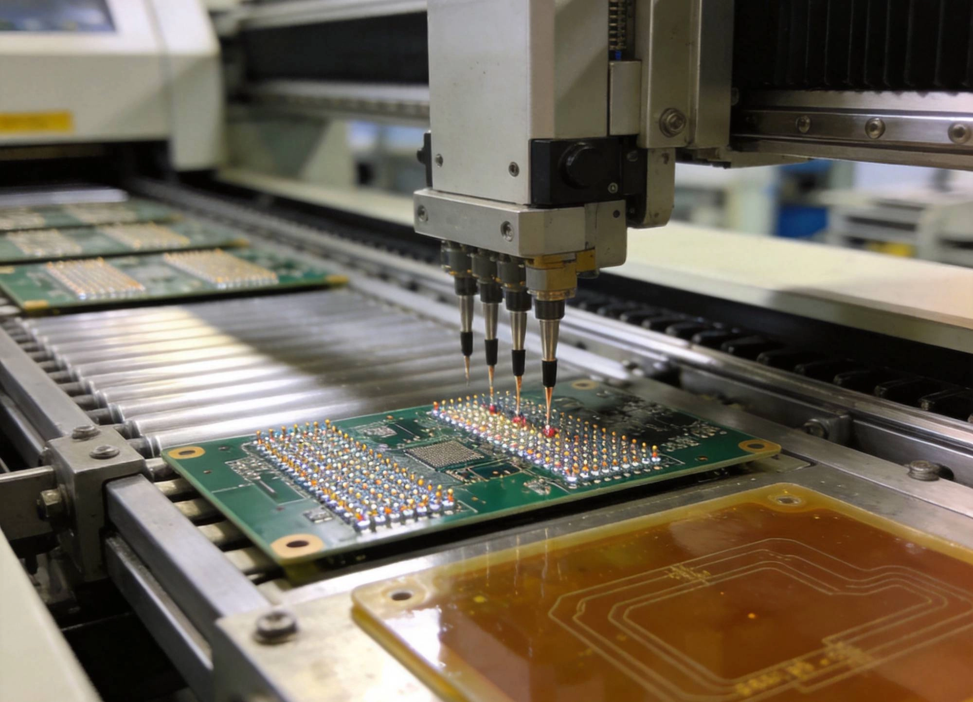
Through-hole technology (THT) dominated electronics assembly from the 1950s through the early 1980s. Components had wire leads that passed through drilled holes in the PCB and were soldered on the opposite side—first by hand, then by wave-soldering machines. THT had clear advantages: the mechanical bond between lead, hole, and solder was robust, and the large component bodies were easy to handle, inspect, and rework by hand.
But THT also had fundamental limitations that became impossible to ignore as electronics shrank:
By the late 1970s, the computer and telecom industries were desperate for higher component density, better high-frequency performance, and faster assembly. The stage was set for SMT.
The earliest surface-mount devices (SMDs) appeared in hybrid microelectronics and calculator manufacturing in the 1970s, but widespread adoption began in the early 1980s, driven by Japanese consumer-electronics makers (Sony, Panasonic, Casio) who needed to miniaturize portable products. Key milestones of this first wave include:
Early SMT lines were hybrid: surface-mount components on the top side, through-hole components on the bottom, with wave soldering for the through-hole side and reflow for the SMT side. This mixed-technology assembly remains common today for boards that include high-power connectors, transformers, or electrolytic capacitors that have no surface-mount equivalent.
The 1990s brought two transformative changes: fine-pitch leaded packages and the first area-array packages (BGAs).
Quad Flat Packages (QFPs) pushed lead pitch from 1.27 mm down to 0.5 mm and eventually 0.3 mm. A 0.5 mm-pitch QFP-208 packed 208 I/Os into a 28 mm square—unthinkable density for through-hole packages. But fine pitch demanded extraordinary process control:
The industry responded with automatic optical inspection (AOI), closed-loop paste-volume measurement, and placement machines with vision-based alignment. These capabilities became permanent fixtures of the SMT line.
Ball Grid Array packages relocated I/O connections from the perimeter to an array of solder balls on the component's underside. A 27 mm × 27 mm BGA-256 offered far more I/O than any QFP at that body size, with shorter interconnects that improved signal integrity at high speeds. BGAs also eliminated the lead-coplanarity problem because the solder balls self-centered during reflow.
But BGAs introduced a new challenge: inspection. The solder joints were hidden beneath the package, invisible to AOI. X-ray inspection became mandatory for BGA assembly, adding equipment cost and throughput constraints. Rework also became harder—removing and replacing a BGA required specialized hot-air rework stations with controlled temperature profiles to avoid damaging adjacent components.
Two forces reshaped SMT in the 2000s: relentless component downsizing and the global transition to lead-free solder.
Passive component sizes collapsed through the decade:
Each step down in size reduced parasitic inductance and capacitance (improving high-frequency performance), saved board area, and lowered per-component cost—but demanded tighter placement accuracy, smaller solder-paste apertures, and more sensitive reflow profiles. A 01005 component weighs roughly 0.1 mg; a slight air draft during placement can blow it off the pad. Handling these parts requires closed-loop vacuum nozzles and vibration-isolated placement heads.
The EU's Restriction of Hazardous Substances (RoHS) directive, effective July 2006, forced the industry away from tin-lead (Sn63Pb37) solder to lead-free alloys, most commonly SAC305 (Sn96.5Ag3.0Cu0.5). The transition affected every aspect of SMT:
The lead-free transition was arguably the most disruptive process change in SMT history, and its effects—especially tin whisker risk in high-reliability applications—are still being managed today.
Smartphones drove the next leap in SMT complexity. A typical 2018-era phone PCB was a 10+ layer HDI board with any-layer microvias, populated on both sides with 01005 passives, 0.4 mm-pitch BGAs, and Package-on-Package (PoP) stacks where a memory die was mounted directly on top of the application processor. PoP assembly required two reflow passes: one for the bottom package, then a flux-dip or paste-print step for the top package before a second reflow. The alignment tolerance between the two packages was ±25 µm—far tighter than conventional SMT placement.
Modern placement machines evolved into dual-gantry, vision-corrected systems capable of placing 80,000+ components per hour with placement accuracy of ±15 µm at 3σ. Features that were optional in the 1990s became standard:
The 2010s also brought the first wave of Industry 4.0 integration into SMT. Machine-to-machine communication (typically via SECS/GEM or OPC UA protocols) enabled:
These capabilities transformed the SMT line from a sequence of isolated machines into a closed-loop, data-driven manufacturing system.
01005 components are now standard in mobile and wearable products. The even smaller 008004 (0.25 × 0.125 mm) has entered pilot production for advanced wearable and medical devices. Placing these parts requires nozzle tips under 200 µm in diameter, sub-10-µm placement accuracy, and reflow profiles tuned to avoid the micro-tombstoning that is prevalent at these pad sizes.
Application processors and baseband chips now routinely use 0.35 mm and 0.3 mm pitch BGAs with 1000+ balls. 0.2 mm pitch is in development for next-generation AI accelerators. At these pitches, solder-paste printing becomes the bottleneck: traditional stencil printing cannot reliably transfer sufficient paste volume to 0.2 mm pads. Solutions include nano-coated stencils, stepped stencils (thinner in fine-pitch regions), and solder-paste dipping for area-array components.
Embedded passives (resistors and capacitors fabricated within the PCB laminate) and embedded actives (discrete dies buried in inner layers) are moving from specialty applications into mainstream automotive and telecom products. Embedding eliminates surface area, reduces parasitic inductance, and improves signal integrity—but requires close collaboration between PCB fabricator and SMT assembler, because embedded components are not inspectable or reworkable after lamination.
Conductive-ink printing and aerosol-jet deposition are emerging as alternatives to etched copper for certain RF and antenna structures. Meanwhile, sintered-copper and transient-liquid-phase bonding offer solder-free interconnects that can survive operating temperatures above 200 °C—a requirement for under-hood automotive electronics and downhole oil-and-gas instrumentation. These technologies are not yet mainstream, but they represent the next evolutionary branch of surface-mount assembly.
Despite five decades of progress, several SMT challenges remain stubbornly unsolved:
For OEMs specifying SMT assembly, the choice of contract manufacturer (CM) is as important as the design itself. Evaluate potential partners on:
The right CM treats your board as their board: investing in design-for-manufacturing (DFM) review before production, flagging warpage risks on large BGAs, and suggesting alternative component packages that improve yield without changing function.
From the first chip resistors soldered onto calculator boards in the early 1980s to today's AI-optimized lines placing 01005 passives and 0.3 mm-pitch BGAs at 80,000 components per hour, Surface Mount Technology has been on a continuous trajectory of densification, speed, and intelligence. Each generation solved the problems of the previous one—only to encounter new challenges at smaller scales and higher frequencies.
The next decade will bring tighter pitches, embedded components, solder-free interconnects, and deeper AI integration across the entire SMT process chain. The fundamentals—solder paste printing, accurate placement, controlled reflow, thorough inspection—will remain, but the precision, speed, and data intensity at which they are executed will continue to advance. Engineers and manufacturers who stay current with SMT's evolution will build smaller, faster, more reliable products. Those who do not will find yesterday's processes unable to assemble tomorrow's designs.
If your project requires SMT assembly at the leading edge of component density and process capability, reach out to our team for a DFM review and production-ready quotation.
SMT components are soldered directly onto pads on the PCB surface without leads passing through holes. Through-hole components have wire leads inserted through drilled holes and soldered on the opposite side. SMT enables smaller components, higher density, better high-frequency performance, and faster automated assembly.
SMT gained significant adoption in the early 1980s, driven by Japanese consumer-electronics companies miniaturizing calculators, radios, and portable devices. Widespread adoption in the West accelerated through the late 1980s and early 1990s.
The 01005 (0.4 × 0.2 mm) is in volume production for mobile and wearable devices. The 008004 (0.25 × 0.125 mm) is in pilot production for advanced applications. These sizes require specialized placement nozzles and sub-10-µm placement accuracy.
Lead-free SAC305 solder requires higher reflow temperatures (~250 °C peak vs. ~220 °C for SnPb), wets more slowly, produces joints that are harder to inspect visually, and introduces tin-whisker risk on pure-tin component terminations. All of these required process, equipment, and reliability adjustments across the industry.
Solder Paste Inspection (SPI) checks paste volume and alignment after printing. Automated Optical Inspection (AOI) checks component presence, polarity, and solder-joint quality after reflow. X-ray inspection is used for hidden joints under BGAs, QFNs, and CSPs. In-circuit testing (ICT) and functional testing verify electrical performance.
High-Reliability PCB Assembly Services for Automotive ElectronicsJuly/08/2026
Low Volume PCB Assembly for Startups The Ultimate GuideJune/03/2026
High-Reliability PCB Assembly Services for Automotive ElectronicsJuly/08/2026
The True Cost of Poor Quality in PCB Assembly ServicesJuly/13/2026

Smart Factories: The Digital Transformation of PCBA LinesSeptember/17/2026