Open Nav



The relentless drive toward smaller, lighter, and more feature-rich electronic devices has pushed manufacturers to adopt increasingly tiny surface mount components. 0201 (0603 metric) and 01005 (0402 metric) components represent the cutting edge of miniaturization in consumer electronics, medical devices, and wearable technology. While these components enable remarkable device downscaling, they introduce significant manufacturing challenges that test the limits of SMT assembly processes. Understanding these challenges is crucial for engineers and product managers working with contract manufacturers in China and beyond.
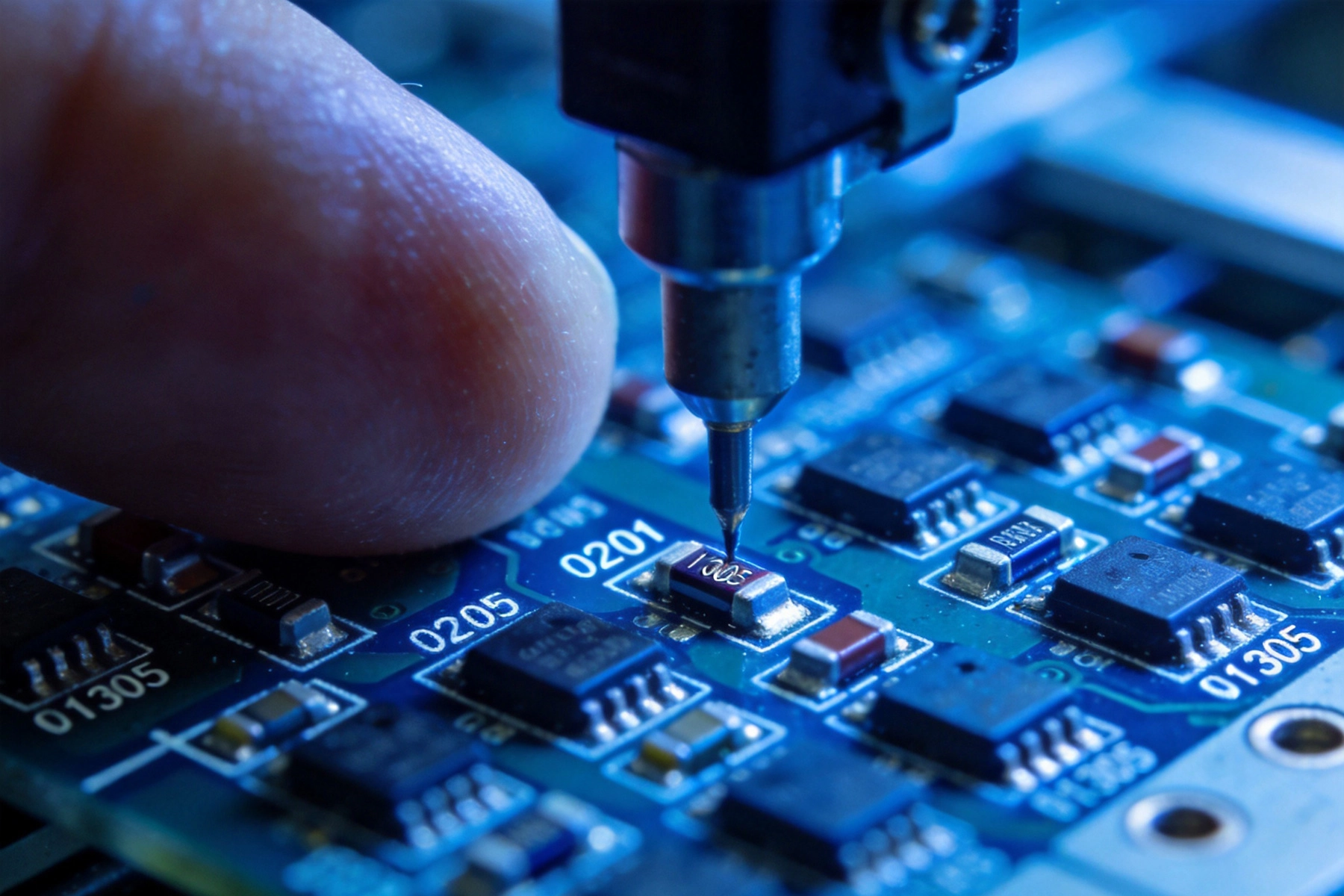
The naming convention for miniature components can cause confusion, particularly when comparing imperial and metric measurements. A 0201 component measures 0.024 inches by 0.012 inches (0.6mm × 0.3mm), while a 01005 component is even smaller at 0.016 inches by 0.008 inches (0.4mm × 0.2mm). To put this in perspective, a human hair averages about 0.003 inches in diameter, meaning a 01005 component is narrower than a single strand of hair.
This extreme miniaturization brings dramatic benefits. A 01005 resistor weighs approximately 0.4 milligrams compared to 16 milligrams for a standard 0805 component. Device manufacturers can place hundreds more components in the same board area, enabling feature-rich products in incredibly compact form factors. However, these benefits come with substantial manufacturing complexity that demands precision equipment and refined processes.
The economics of component miniaturization drive adoption across virtually every electronics sector. Smartwatches, true wireless earbuds, and fitness trackers all rely on 01005 components to achieve their sleek profiles. Medical implants benefit from reduced size enabling less invasive procedures. Smartphone manufacturers pack thousands of tiny components into devices that fit comfortably in pockets. Each generation of product design demands smaller footprints, making 0201 and 01005 assembly skills increasingly essential for competitive contract manufacturers.
The foundation of successful SMT assembly begins with solder paste printing, and this step becomes exponentially more challenging with miniature components. The stencil aperture for a 01005 pad might measure just 0.2mm by 0.1mm, requiring laser-cut stainless steel stencils with exceptional edge quality. Even microscopic variations in paste deposit can cause defective joints.
Stencil thickness selection involves careful trade-offs. Thinner stencils reduce solder volume, helping prevent bridging between adjacent pads, but may not provide sufficient paste for reliable joint formation. Modern manufacturers often use electroformed nickel stencils that offer smoother walls and more consistent paste release than laser-cut alternatives. Nano-coatings on stencil surfaces further improve paste transfer efficiency by reducing surface tension between the paste and stencil walls.
Solder paste characteristics must be optimized for miniature component assembly. Type 6 or Type 7 powder with smaller particle sizes flows more easily into tiny apertures but requires careful handling to prevent oxidation. Print speed typically decreases significantly when printing for 01005 components, as faster speeds can cause paste skipping or incomplete release. Manufacturers must balance throughput requirements against the precision demands of ultra-fine pitch printing.
Closed-loop print verification systems have become essential for high-yield 01005 assembly. These systems use 3D solder paste inspection (SPI) to measure deposit volume, height, and shape after printing. Detecting defects at this early stage prevents wasted components and processing time on boards with insufficient solder for reliable joints.
Pick-and-place equipment faces its own challenges with miniature components. The vacuum pickup tool must generate sufficient suction to lift a component weighing less than half a milligram while avoiding deformation of the tiny body. Standard placement heads designed for 0402 or larger components often lack the precision control needed for consistent 01005 placement.
Modern high-speed placers dedicate specific heads optimized for miniature components. These heads feature finer vacuum control, down-looking cameras for component recognition, and enhanced servo systems that achieve placement accuracies of 15-20 microns at 3-sigma. Despite these specifications, real-world yield rates on 01005 components typically run lower than those for larger parts, making defect detection downstream critical.
Feeding tiny components reliably presents mechanical challenges that compound with miniaturization. 01005 components arrive on tape reels with dramatically reduced pocket sizes, requiring precise servo-controlled feeders that prevent component jumping or ejection during advancement. Vibratory bowl feeders struggle with such small parts, making bulk feeding impractical for most 01005 applications.
Some manufacturers have adopted stick feeders for 01005 components, which offer better component protection and reduced feeding failures. Regardless of feeder type, regular maintenance becomes more frequent and more critical. Worn feeder springs, misaligned guides, and dust accumulation all cause placement defects that would be insignificant with larger components but become catastrophic at the 01005 scale.
The fragile nature of miniature components makes them susceptible to damage throughout the assembly process. Dropped components can become airborne and lost, while excessive pick forces can crack ceramic bodies or damage termination layers. Even normal handling generates electrostatic discharge risks that may not immediately manifest as failures but can cause latent defects appearing weeks or months after product deployment.
Ionized air blowers and ESD-safe work surfaces provide essential protection against electrostatic damage. Operator training emphasizes careful component handling techniques, including proper grip methods and placement procedures that minimize mechanical stress on components. These practices become non-negotiable when assembling 01005 components where defect rates directly impact profitability.
The reflow process presents unique thermal challenges for boards populated with miniature components. 01005 components have minimal thermal mass, meaning they heat and cool faster than larger parts during profile transitions. This faster response can cause incomplete wetting if peak temperatures or liquidus time tolerances are not precisely controlled.
Conversely, adjacent larger components create thermal shadows that protect nearby miniature parts from direct radiant heat. The resulting temperature gradients across a single board can cause some joints to be under-heated while others experience excessive temperatures that damage components or deplete flux activity. Profiling requires multiple thermocouples strategically placed to capture the thermal experience of small components in various board locations.
Void formation in solder joints becomes more problematic with reduced solder volume. A given percentage of void volume represents a larger proportion of total joint volume in 01005 joints compared to larger components. Void concentrations at the interface between component termination and solder can create stress concentration points that lead to mechanical failure under thermal cycling.
Vacuum reflow chambers or specialized void-reducing profiles help address this challenge. Some manufacturers incorporate nitrogen atmosphere reflow that reduces oxidation and improves wetting characteristics. Vacuum-assisted reflow systems actively extract gases during solder melting, achieving void levels below 5% compared to typical 10-20% voids in standard convection reflow.
Detecting defects in 01005 assemblies pushes inspection technology to its limits. Visual inspection becomes impractical as human operators cannot reliably identify issues in components smaller than their visual acuity allows. Automated optical inspection (AOI) systems must achieve resolution and lighting conditions that reveal defects invisible to the unaided eye.
Side-looking cameras and specialized illumination techniques help AOI systems capture 01005 joint geometry. Bright-field and dark-field lighting combinations reveal insufficient paste, misalignment, and tombstoning defects that might be missed with standard inspection setups. However, even advanced AOI systems struggle with certain defect types, particularly head-in-pillow defects where partial wetting creates intermittent electrical connections that pass basic continuity tests.
Some defects hide beneath component bodies where optical inspection cannot reach. BGA packages, QFN components, and even 01005 components with opaque terminations require X-ray inspection to verify joint quality. X-ray systems create images based on material density differences, revealing void content, bridging, and insufficient solder conditions.
Computed tomography (CT) X-ray systems provide three-dimensional inspection capability for critical applications, but the technology remains too slow for production-line inspection of every board. Instead, manufacturers typically sample boards for detailed CT analysis while using faster 2D X-ray systems for production screening of high-risk joint types.
Flying probe testers and in-circuit test systems verify electrical connectivity but struggle with the density of modern 01005 assemblies. Probe tip diameters approach the scale of 01005 pad sizes, making reliable contact challenging. Bed-of-nails fixtures require precision manufacturing and frequent maintenance to maintain contact reliability.
Functional testing becomes increasingly important as a quality verification method, particularly for boards where probe access is limited. While functional test cannot identify all defect types, it catches assembly errors that affect circuit operation and provides confidence that critical parameters fall within specification.
When defects are identified, rework presents significant challenges. Removing a 01005 component without damaging the underlying pads and surrounding components requires exceptional skill and specialized equipment. Hot air rework stations with precision temperature control and small nozzle diameters are essential, but even with proper equipment, successful rework requires experienced technicians.
The risk of collateral damage during 01005 rework is substantial. Excessive heat can lift pads, damage nearby components, or reflow adjacent joints creating new defects. Board flex during heating compounds these risks. Many manufacturers choose to scrap defective boards rather than attempt rework that might introduce additional problems.
The cumulative effect of these challenges translates to higher manufacturing costs for products using 0201 and 01005 components. Equipment investment increases as precision machines replace standard assembly lines. Process development time extends as engineers optimize parameters for acceptable yield rates. Defect rates typically run higher than with larger components, increasing material waste and labor costs.
Despite these costs, the market demand for miniaturized electronics ensures continued adoption of ultra-small components. Manufacturers who master 01005 assembly capabilities gain competitive advantage in high-value product categories where size reduction commands premium pricing. Understanding the challenges helps product designers make informed trade-offs between miniaturization benefits and manufacturing complexity costs.
Contract manufacturers experienced with 0201 and 01005 assembly have developed proven approaches that improve yields and reduce costs. Design for manufacturability (DFM) collaboration between product engineers and assembly specialists identifies potential issues early when corrections cost less. Pad design, component spacing, and thermal relief provisions all influence assembly success.
Process control documentation ensures consistent execution across production runs. Written procedures for stencil maintenance, paste handling, and placement verification maintain quality standards that might otherwise degrade over time or across shifts. Statistical process control tracks key metrics like paste volume variation and placement accuracy, alerting operators to drift before defects become widespread.
Preventive maintenance schedules become more aggressive for equipment processing miniature components. Stencil cleaning intervals shorten to prevent paste accumulation that affects print quality. Feeder calibration checks occur more frequently. Placement head vacuum systems receive regular inspection and adjustment.
Some manufacturers dedicate specific equipment lines to miniature component assembly, avoiding the setup time and contamination risks of switching between component sizes. This dedicated capacity approach increases equipment utilization costs but improves consistency and reduces defect rates that occur during changeovers.
The electronics industry continues pushing toward even smaller components. 008004 (0201 metric) components have entered limited production, representing another step in miniaturization. This trend shows no signs of slowing as Internet of Things devices, medical implants, and wearable electronics demand ever-smaller form factors.
Advanced packaging technologies like embedded components and fan-out wafer level packaging offer alternative paths to miniaturization that may avoid some assembly challenges. However, traditional surface mount assembly will remain relevant for decades as vast manufacturing infrastructure supports this mature technology. Continuous improvement in equipment precision, process knowledge, and inspection capabilities will keep 0201 and 01005 assembly viable for an expanding range of applications.
Assembling 0201 and 01005 miniature components presents genuine manufacturing challenges that demand investment in equipment, process development, and workforce training. Solder paste printing precision, placement accuracy, reflow profile optimization, inspection capability, and rework complexity each require specialized approaches adapted to component miniaturization.
Product teams working with China contract manufacturers should engage assembly partners early in the design phase to benefit from DFM expertise and ensure designs accommodate manufacturing capabilities. Understanding the challenges helps set realistic expectations for yield rates, cost structures, and quality levels. Success in miniature component assembly ultimately rewards manufacturers who invest in the expertise and equipment necessary to compete in miniaturized electronics markets.
Low Volume PCB Assembly: The Bridge Between Prototype and Mass ProductionJuly/07/2026

Inventory Management Benefits of Using a Turnkey Assembly PartnerAugust/03/2026
The Evolution of Surface Mount Technology (SMT) in ElectronicsSeptember/20/2026
The Role of Low Volume Assembly in Aerospace and DefenseJuly/21/2026

The Rise of AI in SMT Quality InspectionJune/18/2026