Open Nav



The rollout of 5G networks represents one of the most demanding manufacturing environments the electronics industry has ever faced. With frequencies pushing into the sub-6 GHz and millimeter-wave bands, the circuit boards that power base stations, active antenna systems, and network core equipment must perform at levels that would have seemed unrealistic a decade ago. For PCB manufacturers and assembly houses, meeting these demands is not just about adopting new materials — it requires rethinking nearly every aspect of the fabrication and assembly process.
This article examines the core challenges facing manufacturers working on 5G infrastructure PCBs, what makes high-frequency assemblies fundamentally different from conventional boards, and the approaches that are proving effective in production.
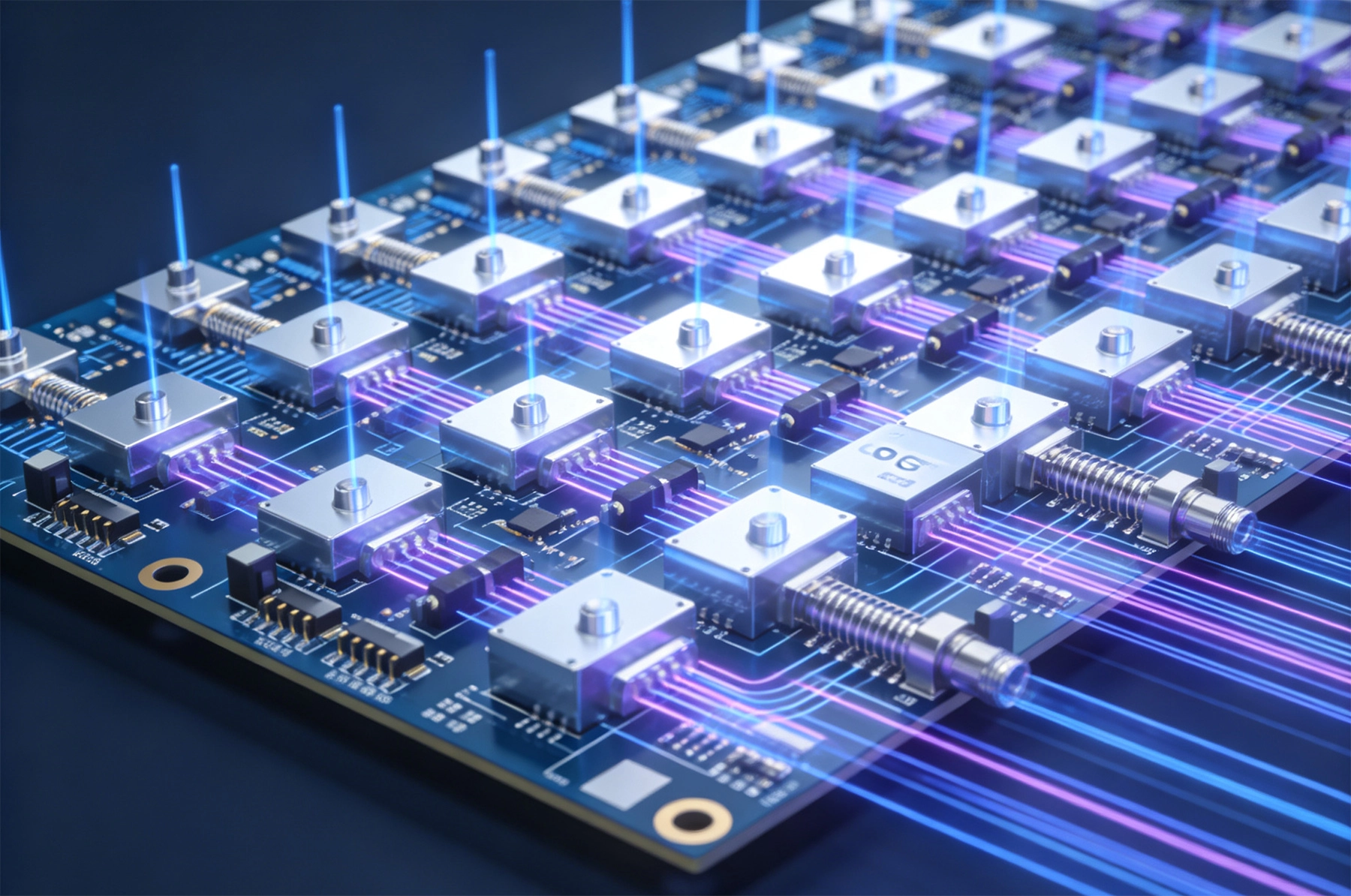
5G operates across a broad spectrum, from low-band frequencies below 1 GHz to mid-band allocations between 3.5 and 6 GHz, up to high-band millimeter-wave (mmWave) frequencies in the 24 to 100 GHz range. Higher frequencies carry more data but are far less forgiving of imperfections. At 28 GHz, a wavelength in free space is roughly 10.7 millimeters. On a PCB trace, the wavelength shrinks further based on the material's dielectric properties — at typical PCB substrate heights, the effective wavelength on a board can be under 5 millimeters.
When trace lengths approach even a small fraction of the signal wavelength, transmission line effects take over. A via that would be completely negligible at 1 GHz becomes a significant discontinuity at 28 GHz. A 0.5 mm routing offset can introduce measurable phase errors. This is the fundamental shift that makes 5G PCB assembly so challenging — the board itself becomes part of the RF system, and every geometric detail matters.
The dielectric properties of the substrate are the primary determinant of signal behavior at high frequencies. Two specifications dominate the conversation: the dielectric constant, known as Dk or εr, and the loss tangent, called Df or tan δ.
The dielectric constant determines the speed at which a signal propagates through the material. Lower Dk values mean faster signal propagation, which is generally desirable for high-speed applications. More critically, the Dk value must be consistent across the board and stable across the operating temperature range. If Dk varies with temperature — a property called Dk drift — the electrical length of a trace changes with thermal conditions, causing frequency response shifts that degrade system performance.
Standard FR-4 materials have Dk values in the range of 4.2 to 4.8, with significant variation across frequency and temperature. For 5G applications, especially in the mmWave band, this variability is unacceptable. Ceramic-filled hydrocarbon laminates and PTFE-based materials offer Dk values between 2.1 and 3.5, with far more stable temperature coefficients. The trade-off is cost, manufacturability, and in some cases, machinability — PTFE in particular requires specialized processing equipment and different handling procedures compared to standard laminates.
The loss tangent determines how much signal energy is converted to heat as it travels through the dielectric. Lower Df means less signal attenuation, which directly translates to better signal integrity and longer effective transmission distances on the board. At mmWave frequencies, even small differences in Df produce measurable performance differences.
For 5G infrastructure operating in the sub-6 GHz range, Df values below 0.005 are generally acceptable. For mmWave applications above 20 GHz, Df should be 0.003 or lower. Achieving this requires careful material specification — not all materials marketed as "high-frequency" actually meet these thresholds, and datasheet values need to be verified against actual test data rather than taken at face value.
Standard PCB substrates use woven glass fiber reinforcement for mechanical strength. At high frequencies, the glass weave pattern creates local variations in Dk across the board — the glass fiber bundles have a different dielectric constant than the resin between them. This effect, known as glass weave resonance or weave periodicity, can cause measurable phase variation across the board surface. At 28 GHz and above, this becomes a significant design and manufacturing concern.
Manufacturers addressing this challenge typically specify spread weave or flat glass styles that reduce the periodic spacing of the weave pattern. Some opt for resin-heavy constructions or even non-woven glass alternatives to minimize the effect. Others use laser ablation or plasma treatment to locally modify the surface Dk characteristics. Whatever the approach, it needs to be validated through impedance testing across the board at operating frequency — impedance measurements at low frequency do not reveal weave effects that become apparent at 28 GHz.
5G PCBs demand precision that pushes the limits of standard fabrication capabilities. Many tolerances that are perfectly acceptable for conventional boards become significant error sources at millimeter-wave frequencies.
High-frequency signal traces are designed for specific characteristic impedance — typically 50 ohms for single-ended routing and 100 ohms for differential pairs. At 28 GHz and above, maintaining impedance within ±5% across the board requires trace width control to tolerances of ±0.5 mils or tighter, combined with precise control of dielectric thickness. Standard PCB Fabrication processes with tolerances of ±1 to 2 mils on trace width cannot consistently meet these requirements without process improvements specifically targeted at impedance control.
This means tighter incoming inspection of base copper thickness, tighter control of etching parameters, and statistical process control throughout the production run rather than inspection-based end-of-line testing. Some manufacturers run impedance test coupons on every panel and track trends in real time, adjusting process parameters before out-of-spec boards are produced rather than catching them after.
Vias are one of the most problematic structures in high-frequency PCB design. A through-hole via creates an impedance discontinuity — the signal sees a change in geometry as it transitions from a trace to a via barrel and back to a trace. At 1 GHz, this discontinuity is negligible. At 28 GHz, it can produce significant return loss and signal distortion.
The standard mitigation is via back-drilling — removing the unused portion of the via barrel beyond the signal layer to reduce the stub length that causes resonance. For 5G boards, via back-drilling tolerances need to be tighter, and the drilled barrel wall quality must be consistent. Residual stub lengths of even 5–10 mils can cause measurable degradation at mmWave frequencies.
Alternative via structures like blind vias, buried vias, and via-in-pad require their own evaluation. Each introduces its own impedance discontinuity characteristics that must be modeled and tested. The via design for a 28 GHz antenna feed network is a far more critical engineering decision than the same decision for a 1 GHz board.
5G base stations and active antenna systems dissipate significant power continuously. The power amplifiers, beamforming ICs, and network processors in a typical 5G macro cell can generate tens to hundreds of watts of heat that must be managed without degrading PCB performance. For high-frequency materials, thermal management is complicated by the fact that many high-Dk and low-loss materials have worse thermal conductivity than standard FR-4.
PTFE laminates, which are among the best performers from an electrical standpoint, have thermal conductivity around 0.25 W/m·K — roughly 1/8th that of aluminum. This means heat does not spread easily through the board substrate, and local hot spots can develop directly under high-power components.
Effective thermal management for 5G assemblies typically involves metal-core substrates, thermal vias under major heat sources, and sometimes direct liquid cooling integration in the most demanding deployments. The PCB designer needs to coordinate thermal and electrical requirements from the start — treating them as separate disciplines is a recipe for expensive redesigns. Assembly manufacturers need to understand thermal constraints well enough to flag potential issues during design review, not discover them during reliability testing.
Fabricating a 5G PCB to the right specifications is only half the battle. The assembly process introduces its own set of challenges that can degrade performance if not properly controlled.
High-frequency signal traces are extremely sensitive to surface irregularities. The skin effect at mmWave frequencies means current concentrates on the surface of the conductor — any roughness in the copper surface increases effective resistance and creates scattering losses. Standard HASL (Hot Air Solder Leveling) finishes, with their characteristic irregular surface, introduce measurable loss at 28 GHz and above. ENIG (Electroless Nickel Immersion Gold) provides a smoother surface and is generally preferred for high-frequency applications, though the gold thickness must be controlled — too thick a gold layer introduces its own problems.
Solder paste selection also matters. Voiding — air bubbles trapped in solder joints — creates local thermal and mechanical inconsistencies. For high-power components, void content above 10% can cause meaningful thermal performance degradation. For 5G assemblies, void content targets are typically set at 5% or lower, requiring void-reducing solder paste chemistries and optimized reflow profiles.
The placement accuracy requirements for 5G assemblies are significantly tighter than for conventional boards. Misalignment of a mmWave passive component by even 1 mil relative to the designed land pattern can cause measurable impedance deviations. This requires assembly equipment with tighter pick-and-place accuracy specifications and vision systems capable of compensating for board warpage and fiducial recognition at high resolution.
For antenna array modules operating at 28 GHz or higher, placement accuracy requirements can be measured in microns. These assemblies are often produced using advanced packaging techniques like fan-out wafer-level packaging (FOWLP) or precision chip-on-board assembly, where the standard SMT reflow flow is not sufficient.
At high frequencies, electromagnetic interference becomes far more difficult to contain. The wavelength at 28 GHz is approximately 11 mm, meaning even small gaps in shielding enclosures can act as slot antennas, allowing radiation to escape and couple into adjacent circuits. Board-level shielding techniques — metal cans, conductive gaskets, via fences — must be designed with frequency-appropriate clearance and grounding. Assembly manufacturers must ensure that shield contact points are clean, compressed correctly, and maintain contact integrity over the product's operational life.
Testing a 5G PCB assembly is fundamentally different from testing a conventional board. Low-frequency continuity and insulation resistance tests tell you almost nothing about high-frequency performance. You need RF test capabilities, and those capabilities are expensive and require specialized expertise to operate correctly.
A Vector Network Analyzer (VNA) is the primary instrument for characterizing high-frequency PCB performance. It measures S-parameters — specifically S21 (insertion loss) and S11 (return loss) — across the frequency range of interest. For 5G boards, VNA testing should cover at minimum the full operating frequency range, from DC to 10% above the maximum intended operating frequency.
VNA testing requires proper calibration using appropriate calibration standards and test fixtures. The quality of the test setup — including cable care, connector torque, and board fixturing — directly affects measurement accuracy. Many manufacturers discover that their first VNA measurements are unreliable until they invest in proper calibration procedures and test equipment maintenance.
5G infrastructure equipment is expected to operate reliably in outdoor environments for 20 years or more. This requires extensive accelerated life testing, including thermal cycling across the full operating temperature range, humidity exposure, vibration testing, and combinations of these stressors. For high-frequency assemblies, the critical failure mode to watch for is not just electrical opens or shorts — it is drift in RF performance parameters like insertion loss and return loss over temperature cycling. A board that passes all DC tests but shows increasing loss at 28 GHz after 500 thermal cycles has a real reliability problem, even though a standard ICT would report it as good.
Manufacturing PCBs for 5G infrastructure is not a capability you add casually. It requires coordinated investment across multiple domains:
5G infrastructure PCB assembly sits at the edge of what current manufacturing technology can reliably produce. The combination of high frequency, tight tolerances, demanding thermal environments, and long reliability requirements creates a set of challenges that is qualitatively different from conventional PCB work. Manufacturers who invest in the right materials, process controls, test capabilities, and engineering expertise are positioning themselves for a market that will grow substantially as 5G networks continue their global expansion.
The barriers to entry are high, but so is the value of the capability. For manufacturers already in the supply chain and for those considering entry, the message is clear: 5G PCB assembly rewards rigor and punishes shortcuts. The boards that will power the next generation of wireless infrastructure need to be built right, and that requires taking every challenge seriously.
Contact us to discuss your requirements.
Designing for Testability (DFT): Ensuring Quality in Mass ProductionOctober/13/2026

The Role of Low Volume Assembly in Aerospace and DefenseJuly/21/2026
Top 10 DFM (Design for Manufacturability) Tips for SMT PCB AssemblyJune/08/2026

Full Turnkey Solutions: Simplifying Your Supply Chain ManagementSeptember/09/2026
Avoiding Tombstoning and Bridging in Your PCB LayoutJuly/30/2026